ULTRA LIBRARIAN: GLOSSARY

PCB DESIGN TERMINOLOGY

UNDERSTANDING BASIC TERMINOLOGY IS KEY TO SUCCESS IN THE PCB INDUSTRY

PCB design software and the electronic components industry have come together to drive much of the terminology used by professional designers and engineers. For new designers and engineers, understanding the basic terminology involved in PCB design eases the curve involved in learning ECAD software and helps designers communicate with systems engineers, component vendors, and manufacturers.

Electronic Circuit Board
GLOSSARY

The glossary shown here is divided up into two sections—one section covers terminology used in ECAD software and the other section covers terminology used to describe board construction and the physical layout of the board.

ECAD TERMINOLOGY

PCB layout

A CAD document showing the location of all physical elements that will appear on the finished PCB.

Schematic sheets

Functional drawings that illustrate the electrical connections between components.

Ultra Librarian Chip Icon

Fun Fact

Schematic design is sometimes called logic creation, referring to the use of logic components in DIP packages to perform logic operations before the advent of heavily integrated processors and microcontrollers.

SPICE

Stands for “Simulation Program with Integrated Circuit Emphasis”; a simulation package that solves Kirchhoff’s laws for circuit diagrams using a numerical algorithm.

Component

Functional drawings that illustrate the electrical connections between components. A CAD object that defines how a real electronic component is represented in schematic sheets and a PCB layout in ECAD software. All components include a schematic symbol and PCB footprint that are used to create schematics and a PCB layout, respectively. A component may also include a SPICE subcircuit for use in circuit simulations, and a 3D model for use in MCAD software.

Schematic Symbol

A box with drawn leads that represent the physical leads on a component. The leads in a schematic symbol are used to make electrical connections in schematic sheets.
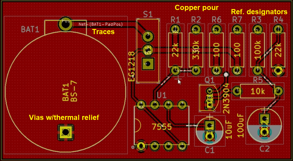
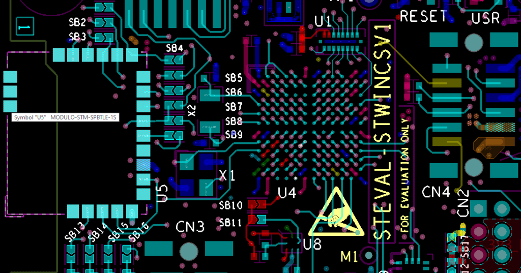
PCB Footprint

A CAD object that includes the land pattern, silkscreen outline, and package mechanical outline.

SPICE subcircuit

An ASCII-based simulation file that describes the electrical behavior of a component in SPICE simulations.

Component library or PCB library

A component library (or, simply, library) includes multiple components in a single file or set of files. Libraries are needed to create CAD documents in ECAD software, and the software will pull data from the libraries.
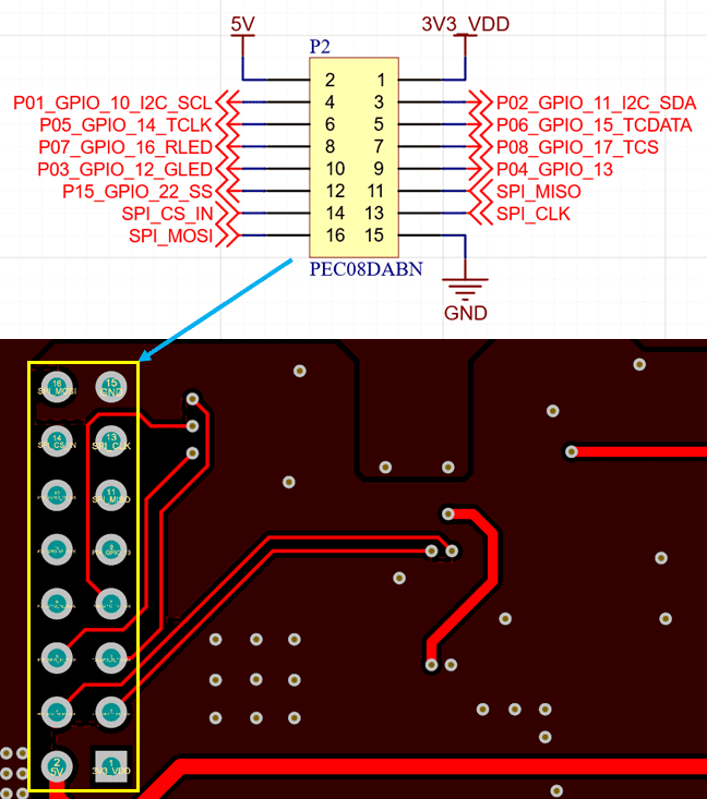
Nets

A graphical connection between two components that represents an electrical connection on a manufactured circuit board.

Schem PCB

Nets in the schematic correspond to physical connections in the PCB layout

Reference Designator

An alphanumeric code that is used to denote specific components in a PCB layout and schematic (example: U4 or C35). The letter prefix corresponds to a type of component and numbers are assigned to each type of component in series. 

Interconnect

The general name given to an electrical connection between two components. This can be inclusive of all nets on the PCB, connectors, vias (see definition below), or other media used to make a physical connection in an electronic system.

High density interconnect (HDI)

A type of PCB where trace widths are very small (usually 4 mil or less) and layer counts tend to be very high (typically 12 or more). HDI PCB design normally requires the use of microvias (see definition below) to make connections between layers.

Design for manufacturing (DFM)

A practice where a design considers how the product will be fabricated and where fabrication constraints are used as design rules in ECAD software.

Design for assembly (DFA)

A practice where assembly constraints are considered during design and are defined in ECAD software as design rules.

Design for testability (DFT)

Typically used for prototype design, this design practice emphasizes inclusion of features that enable the collection of electrical measurements and quality inspection.

Ultra Librarian Chip Icon

Fun Fact

The three terms above are sometimes lumped together into a larger idea known as DFX, or “design for X”, due to the application of these principles beyond manufacturing, assembly, and testing.

BOARD CONSTRUCTION AND PHYSICAL LAYOUT

When we refer to “board construction”, we’re not just talking about something that happens in manufacturing. ECAD software companies and designers use many of the same terms as manufacturers to describe the features in a CAD layout, as well as their corresponding features on a fabricated circuit board. Here are some of the important terms used to describe a physical PCB layout.

PCB stackup

Sometimes called a layer stack, this refers to the arrangement of layers used to construct the PCB. The PCB stackup is created in your ECAD software before creating the PCB layout.

PCB laminate

Generally refers to any material used to create each layer in a PCB stackup.

Core and prepreg

Two forms of a PCB laminate material. The core refers to a laminate sheet with copper on both sides and the prepreg is used as a bonding layer.

FR4

Refers to a class of PCB laminate materials that have a Class 4 NEMA flammability rating. These are standard materials used to build PCBs.

Rogers

A popular series of high frequency PCB laminate materials that are commonly used in RF/wireless systems.

Signal and plane layers

Two types of layers in a PCB stackup. Plane layers have a complete layer of copper covering the entire laminate, while signal layers are etched with traces, polygons, and other copper features.

Traces and polygons

Two principal copper features on a printed circuit board. Traces connect the pads on component land patterns, while polygons are used to fill in the space between traces with copper to provide grounding and shielding. A trace is also called a track.
KiCAD Layout

Copper pour, traces, vias, and reference designators in a KiCAD PCB layout.

Ultra Librarian Chip Icon

Fun Fact

A polygon is often called a polygon pour or copper pour. Filling in the empty space on a PCB with grounded copper provides shielding against EMI.

Pad

Used with SMD components, a pad is where the component will sit and provides a point where solder can be applied.

Vias

A hole with copper plating along the axis that is used to route signals between multiple layers. Vias can also be non-plated. Types of vias include through-hole, buried, blind, and microvias.

Via-in-pad plated-over (VIPPO)

A via style where the via is placed in the pad for a component and plated over with copper. To ensure complete coverage of the via, the via may be filled with an epoxy or it may be totally filled with copper.

Microvia

These vias are very small (about less than 6 mil diameter) and are used in HDI PCB design to route signals between layers.

Annular ring

The leftover area of a copper pad around a drilled and finished hole.

Thermal vias

A via connected back to a plane layer, which is meant to dissipate heat from a high-power component.

Thermal relief

This is sometimes confused with a thermal via, but they are not the same. A thermal relief is generally placed on a via that makes a connection between a solder pad and a plane layer. Thermal reliefs help ensure strong solder is brought to the correct temperature during assembly.

Solder mask

The top layer of a printed circuit board that gives the board its distinctive color. Green is probably the most popular color, although almost any color solder mask can be used.

Via tenting

A practice where a via is covered with a solder mask to prevent molten solder from wicking to the back layer during assembly.

Silkscreen

The layer used to print reference designators, text, logos, and any other information on top of the solder mask on a fabricated circuit board.
Cadence Layout

This layout image in Cadence Allegro shows the top copper layer and top silkscreen for the STEVAL-STWINKT1B reference design from STMicroelectronics

Land pattern

Refers to the size of pads, arrangement of pads, and package outline for a given part that should be designed onto a PCB. Land patterns for standard component packages are defined in the IPC-7351B standards (SMD components) and IPC-7251 standards (through-hole components).

Ultra Librarian Chip Icon

Fun Fact

The terms land pattern and PCB footprint are sometimes used interchangeably, but they are technically not the same thing. A component could have several allowable land patterns, but it will only have one footprint.

Surface-mount technology (SMT) or surface-mount device (SMD)

Refers to electronic components that are mounted directly to pads on a surface layer.

Through-hole technology

Refers to electronic components that are mounted to a PCB by placing leads into through-hole vias.

USE ULTRA LIBRARIAN'S ELECTRONIC SEARCH ENGINE FOR YOUR DESIGN NEEDS

At Ultra Librarian, we care deeply about the success of all PCB designers and engineers, and we strive to provide resources to help new designers advance their careers. In addition to our glossaries, one of the resources we provide is a comprehensive electronics search engine that helps designers find the components they need. All Ultra Librarian users can access CAD models for components and verified 3D models that can be imported into popular ECAD applications. We also give users access to aggregated sourcing information from worldwide distributors.

Through Hole Component

These axial resistors are classic through-hole components

Ultra Librarian Chip Icon

Working with Ultra Librarian sets up your team for success to ensure streamlined and error-free design, production, and sourcing. Register today for free.