


USB Power Delivery buck boost DC-DC converter for automotive application is used to power USB PD-enabled devices such as smartphones, tablets, and other electronic devices.
Power Regulation is one of the most challenging issues for engineers when designing for automotive applications. Toshiba Devices & Storage Corporation, an industry leader in building electronic systems for many challenging applications; including automotives, has developed a solution that addresses this need. The design couples USB Power Delivery (USB PD) with buck boost topology to effectively regulate and convert power in automotive environments.
The Automotive Buck-Boost DC-DC Converter for USB PD is used to power USB PD-enabled devices, such as smartphones, tablets, and other electronic devices. This converter ensures reliable and efficient charging of USB PD devices by providing the voltage and current levels they need. Using buck boost topology, the converter can step up (boost) or down (buck) the input voltage to provide the desired output voltage. Due to fluctuations in the vehicle’s electrical system, this flexibility is essential.
Key Features for a USB Power Delivery Buck Boost DC-DC Converter
Key features of a USB PD buck boost DC-DC converter for automotive applications include:
- Input voltage range: The converter supports a wide input voltage range to accommodate the varying electrical conditions in automotive systems (e.g., 5V to 18V).
- Output voltage range: The converter generates multiple output voltage levels, such as 5V, 9V, 15V, and potentially higher voltages required by USB PD devices.
- USB PD support: The converter complies with the USB PD specification, enabling it to negotiate power profiles and deliver higher power levels.
- Efficiency and power handling: The converter is designed for high efficiency to minimize power loss and maximize charging speed. It can handle the power levels required by USB PD devices (e.g., 15W, 27W, 45W, or higher).
- Protection and safety features: The converter incorporates protection mechanisms to safeguard against overvoltage, overcurrent, and short circuits, ensuring the safety of the connected devices and the vehicle’s electrical system.
- Automotive-grade specifications: The converter meets automotive industry standards for reliability, temperature range, and other environmental factors encountered in vehicle applications.
- EMI/EMC compliance: The converter complies with electromagnetic interference (EMI) and electromagnetic compatibility (EMC) standards to minimize potential interference with other vehicle electronics.
To fully take advantage of these features, certain considerations must be incorporated into your design.
PCB Design Considerations for USB PD Buck Boost DC-DC Converter
There are several PCB design considerations regarding the USB PD buck boost DC-DC converter for automotive applications, as shown in the table below.
|
USB PD Buck Boost DC-DC Converter for Automation Application: PCB Design Considerations |
|
|
Layout |
Input and output connections, heat dissipation, signal integrity, and component placement |
|
High Current Traces |
Wider and thicker traces to carry increased current |
|
Thermal Management |
Thermal vias, heatsinks, and copper pours to dissipate heat |
|
EMI/EMC Considerations |
Proper grounding, shielding, and routing techniques |
|
Power and Signal Isolation |
Isolation of power circuitry from the rest of the PCB |
|
Component Placement |
Signal path lengths minimization, noise coupling reduction, and thermal dissipation and safety clearances |
|
Input/Output Filtering |
Filtered input and output connections |
|
Safety Considerations |
Overvoltage protection, overcurrent protection, and short-circuit protection |
Addressing PCB Design Considerations
The PCB design considerations for the USB PD buck boost DC-DC converter for automation applications listed above can be addressed by following the guidelines below.
Guidelines for USB Power Delivery PCB Design
Layout: The converter must be carefully placed and routed on the PCB to ensure efficient power delivery and minimize noise and interference. The PCB designer should consider the converter’s input and output connections, heat dissipation, signal integrity, and component placement.
High Current Traces: USB PD converters can handle higher currents in fast-charging applications. For this reason, wider and thicker traces are required to carry increased current without causing voltage drops or overheating. For optimal performance and to prevent excessive heating, copper thickness and trace width must be maintained properly.
Thermal Management: The thermal management of power converters is crucial in automotive environments where temperatures may fluctuate. PCBs should be designed to dissipate heat effectively and prevent overheating using thermal vias, heatsinks, and copper pours.
EMI/EMC Considerations: Due to high-frequency switching, USB PD converters can generate electromagnetic interference (EMI). The PCB layout should be carefully designed to minimize EMI emissions and comply with electromagnetic compatibility (EMC) standards. Proper grounding, shielding, and routing techniques are required for noise reduction and interference reduction.
Power and Signal Isolation: To protect sensitive components or circuits, isolating the converter’s power circuitry from the rest of the PCB may be necessary. A PCB design may need to incorporate isolation techniques such as optocouplers or transformers.
Component Placement and Clearance: The placement of components, such as capacitors, inductors, and control ICs, should minimize signal path lengths, reduce noise coupling, and ensure thermal dissipation and safety clearances.
Input and Output Filtering: Input and output connections must be properly filtered to reduce noise, stabilize voltage levels, and prevent conducted and radiated interference. Filter components such as capacitors, inductors, and ferrite beads may be used to suppress unwanted noise and maintain signal integrity.
Safety Considerations: There are stringent safety requirements in automotive applications. The PCB design needs to comply with safety standards and incorporate features such as overvoltage protection, overcurrent protection, and short-circuit protection. Isolation techniques and fuse placement should also be considered.
Following the guidelines above will aid you in designing an automotive system power delivery solution that meets your functional and operational objectives. However, by utilizing components and a layout architecture that specifically targets power supply and regulation automotive electronics you can achieve an optimal USB PD circuit design.
Optimizing Your USB PD Circuit Design
The best USB PD design begins with your component selection. Sourcing high-quality components from a trusted supplier with a proven track record for designing and manufacturing high-performance and reliable parts, such as Toshiba is the answer. An advanced USB PD buck boost DC-DC converter reference design driven by Toshiba components is shown below.
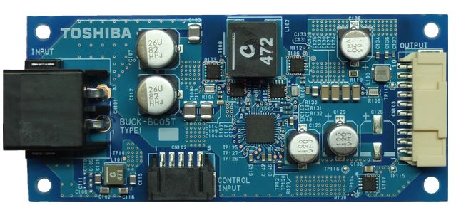

High-performance USB Power Delivery buck boost DC-DC converter reference design for automotive application driven by Toshiba components.
This reference design includes the following key components:
|
Components |
Device Type (Quantity) |
Usage |
Specifications |
|
Power MOSFET (4) |
H-Bridge Switch |
N-ch, 40 V, 20 A, 0.0071 Ω@10V, TSON Advance (WF) packaging |
|
|
Small Low ON Resistance MOSFET (4) |
H-Bridge Switch |
N-ch, 40V, 12A, 18 mΩ@4.5V, TSOP6F packaging |
|
|
Power MOSFET (3) |
Switch |
N-ch, 40 V, 40 A, 0.0038 Ω@10V, TSON Advance(WF) packaging |
|
|
Intelligent High-side MODFET Driver (1) |
Gate Driver |
Automotive Gate driver for High-side switch, PS-8 packaging |
The components listed above are essential elements for the USB PD buck boost DC-DC converter reference design above. In addition to satisfying the USB PD converter requirements, this parts package has the following favorable attributes:
✅ Small package MOSFETs that require minimal surface area, which simplifies routing.
✅ High efficiency power supply with low heat dissipation requirements.
✅ Wide range of temperature operation.
It is important to consult the datasheet, application notes, and guidelines provided by the component manufacturer to understand specific PCB layout and design recommendations for their product. However, optimal USB PD converter design optimization begins with selecting the best components for your product from a reliable source. Doing so pouts you on the road to success for ensuring that your USB PD converter design will operate reliably in the often harsh automotive systems environment.
If you’re looking for CAD models for common components or a USB Power Delivery buck boost DC-DC converter for automotive applications, Ultra Librarian helps by compiling all your sourcing and CAD information in one place.
Working with Ultra Librarian sets up your team for success to ensure streamlined and error-free design, production, and sourcing. Register today for free.