

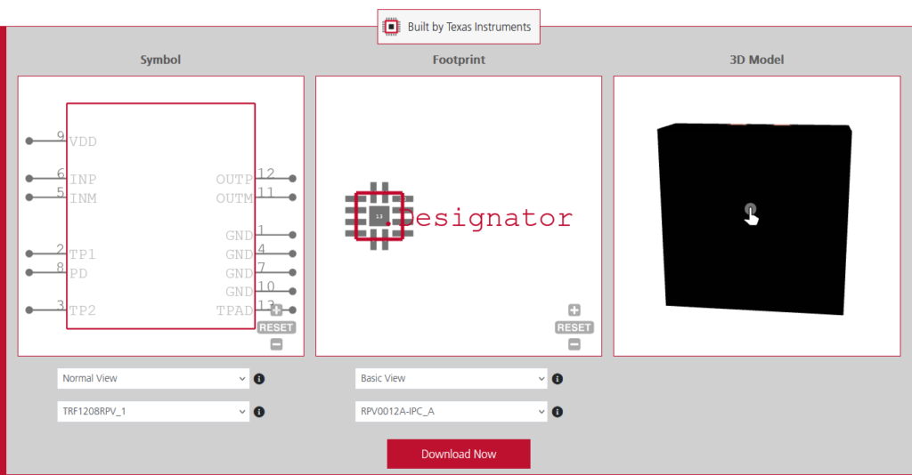


TRF1208 Symbol, Footprint, and 3D Model on Ultra Librarian
In the high-stakes world of Radio Frequency (RF) and high-speed data acquisition, the signal chain is only as strong as its weakest link. As Analog-to-Digital Converters (ADCs) push toward higher sampling rates and wider bandwidths, the amplifiers driving them must keep pace. Enter the Texas Instruments TRF1208, an ultra-wideband, high-performance differential amplifier designed specifically to act as the bridge between RF signals and high-speed data converters. This article breaks down the TRF1208 datasheet to highlight its core specifications, pinout architecture, and typical application strategies.
Understanding Differential Amplifiers and the TRF1208
Differential amplifiers are designed to amplify the difference between two input signals while rejecting common-mode noise. This ability makes them essential in applications requiring high accuracy, low noise, and strong interference rejection, such as sensor interfaces, communication systems, and signal conditioning circuits.
The Texas Instruments TRF1208 represents a high-performance evolution of this concept. It is an ultra-wideband differential amplifier specifically engineered to interface directly with high-speed Analog-to-Digital Converters (ADCs). With a bandwidth from 10 MHz to 11 GHz, the TRF1208 preserves wideband RF signal content as it moves into the digital domain. It delivers a clean, well-balanced differential output that high-speed ADCs require for accurate conversion. By performing this conditioning and translation, the TRF1208 acts as a bridge between raw RF signals and digital processing, enabling applications such as 5G infrastructure, phased-array radar, and precision test instrumentation.
TRF1208 Datasheet Core Specifications
The TRF1208 is distinguished by its ability to operate from DC up to extremely high frequencies (11 GHz) while maintaining signal integrity. It is designed to drive the input of high-speed ADCs, converting single-ended signals to differential or buffering differential signals. The device is built to minimize distortion, which is important for preserving the dynamic range of the downstream ADC.
Key Technical Specifications
| Specification | Typical Value / Range |
| Bandwidth (-3dB) | 10 MHz to 11 GHz |
| Gain | 16 dB |
| Noise Figure | 7 dB (@ 2 GHz) |
| Output IP3 (OIP3) | 42 dBm (@ 2 GHz) |
| Supply Voltage | 3.3 V or 5 V |
| Power Consumption |
Pin Configuration and Functions
The TRF1208 comes in a compact 2mm × 2mm, 12-pin WQFN package. Understanding the pinout is crucial for layout, as the symmetry of the input and output pins directly impacts the balance of the differential signal.
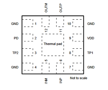

Pin configuration diagram of the TRF1208 (Top View) showing differential inputs and outputs.
TRF1208 Pin Descriptions
| Pin Name | Pin No. | Type | Description |
| GND | 1, 4, 7, 10 | GND | Ground connection. |
| PD | 2 | Input | Power-down signal. Supports 1.8-V and 3.3-V Logic.<br>0 = Chip enabled<br>1 = Power down. |
| TP2 | 3 | – | Test pin. Short to ground. |
| INM | 5 | Input | Differential signal input, negative. |
| INP | 6 | Input | Differential signal input, positive. |
| TP1 | 8 | – | Test pin. Short to ground. |
| VDD | 9 | Power | 3.3-V supply. |
| OUTP | 11 | Output | Differential signal output, positive. |
| OUTM | 12 | Output | Differential signal output, negative. |
| Thermal Pad | Pad | – | Exposed thermal pad. Connect to ground on the board for thermal dissipation. |
Typical Application: ADC Driver
The primary use case is driving a high-speed ADC, such as the TI ADC12DJ3200 or ADC12DJ5200RF. In this configuration, the TRF1208 acts as both a buffer and a gain block, isolating the ADC from upstream RF circuitry while scaling the signal to fully utilize the converter’s input range without introducing distortion.
The amplifier is typically AC-coupled at both the input and output. The TRF1208 datasheet recommends specific balun configurations if converting from single-ended to differential. A key aspect of the application circuit is the matching network. Because the TRF1208 operates in the GHz range, the input and output traces must be treated as transmission lines (typically 50Ω or 100Ω differential), and components must be selected to match the impedance of the ADC input filter.
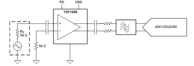

Typical schematic showing the TRF1208 driving a high-speed ADC with AC coupling capacitors.
Layout Considerations for High-Frequency Performance
At 11 GHz, the PCB layout is as important as the schematic. The datasheet emphasizes several critical layout practices:
- Symmetry: The differential input and output traces (IN+/IN- and OUT+/OUT-) must be routed symmetrically to maintain phase balance and reject common-mode noise.
- Grounding: The exposed thermal pad must be soldered to a solid ground plane with multiple thermal vias to ensure heat dissipation and a low-inductance ground return.
- Decoupling: Power supply bypass capacitors must be placed immediately adjacent to the VCC pin to prevent high-frequency noise from coupling into the amplifier.
The TRF1208 is a powerful component for modern RF front-ends, offering the bandwidth and linearity required for next-generation communications and radar applications. When designing with high-frequency components like the TRF1208, having accurate CAD data is non-negotiable. An incorrect footprint pad size can alter impedance, and a missing thermal via can lead to overheating.
If you’re looking for verified CAD models for the TRF1208 datasheet, Ultra Librarian helps by compiling all your sourcing and CAD information in one place. Our platform provides verified, ready-to-use footprints, symbols, and 3D models that support all popular ECAD applications, along with sourcing information from worldwide distributors.
Working with Ultra Librarian sets your team up for success, ensuring streamlined and error-free design, production, and sourcing. Register today for free.