

If you need a diode for rectification that admits current with low forward voltage and fast switching speed, then a Schottky diode is the standard option. These characteristics make Schottky barrier rectifiers useful in power delivery to wave shaping applications. In this article, we’ll look at how these components stack up to their p-n diode cousins and when you might best be served using a Schottky barrier rectifier instead.
About Schottky Barrier Rectifiers
In the most basic sense, a Schottky barrier rectifier (or simply Schottky diode) operates in the same manner as a typical semiconductor diode made from Si or Ge. However, its primary purpose is to provide rectification, i.e., allow current to flow only easily along one specific direction. In this way, they are used in typical DC circuits to enable or block current or in AC circuits as part of wave shaping.
Structure
The major differences between a Schottky diode include their forward operating characteristics and, most importantly, their structure. Schottky diodes are constructed by depositing a metal electrical contact on a semiconductor; although n-type or p-type materials can be used in Schottky diodes, n-type materials are normally preferred. The reason is that p-type semiconductor Schottky diodes will have lower forward voltage and thus larger reverse bias breakdown current; using an n-type material provides the best balance between forward voltage and reverse bias current. On the other ends of the component, Ohmic contacts are placed to provide non-rectifying connections to the semiconductor.
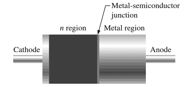

Schottky barrier rectifier structure.
Advantages of Schottky Diodes
Compared to p-n junction diodes, Schottky barrier rectifiers have some advantages that make them more useful in switching, high-frequency rectification, and wave shaping applications. Some of the main advantages of Schottky diodes include:
- Narrow depletion region: When forward biased, a Schottky diode will have a smaller depletion region than in a p-n diode. As a result, the junction capacitance is very low, and a Schottky diode can be switched between forward and reverse biases very quickly.
- Lower forward voltage: A Schottky diode’s forward voltage is determined by its built-in voltage, which can be as low as 0.2 to 0.3 V. For comparison, Si p-n diodes have forward voltages of approximately 0.6 to 0.7 V, so they produce less current in forward bias.
- Low ideality factor: Schottky diodes tend to have low ideality factor, with values as low as 1.04 being common in commercially available components.
- Less noise: A Schottky diode will have lower nonlinear impedance in forward bias, producing less unwanted thermal noise than a typical p-n junction diode. This is one reason Schottky diodes are useful in microwave devices.
As shown below, the electrical advantages can be seen when comparing IV curves for a Si p-n diode and a Schottky diode. From here, we can see that the larger reverse bias current behavior leads to slower roll-off into the breakdown region, rather than fast avalanche behavior seen in a p-n diode.
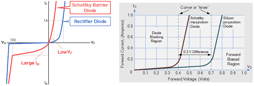

IV curves (left) and forward voltage behavior (right) for Si p-n diodes and Schottky diodes.
Typical Uses of Schottky Barrier Rectifiers
The three major application areas for Schottky barrier rectifiers include switching converters for power regulation, ESD protection, and in microwave circuits. Both applications place requirements on three specifications: the junction capacitance (determines the recovery time and frequency response), voltage limit, and current limit.
Power Conversion
In power systems, Schottky diodes are switched between forward bias and reverse bias in order to direct a DC current across an inductor and to the output of a regulator circuit. The diode needs to switch and fully modulate between the two states at the same rate as the driving PWM signal in the upstream switching power MOSFETs, which requires low junction capacitance. The other two important specifications are the voltage and current limits; the device should be able to provide rectification at the applied voltage during operation without entering breakdown.
Microwave Circuits
Schottky diodes can be used in microwave circuits that operate up to GHz frequencies in low-load conditions. The recovery time will be limited by the load impedance and the junction capacitance (see below for an example in a 1N5822 Schottky diode). One big advantage of a Schottky diode in microwave circuits compared to a Si p-n diode is its linearity near zero bias, allowing oscillating signals to be collected directly, and without DC offset if needed.
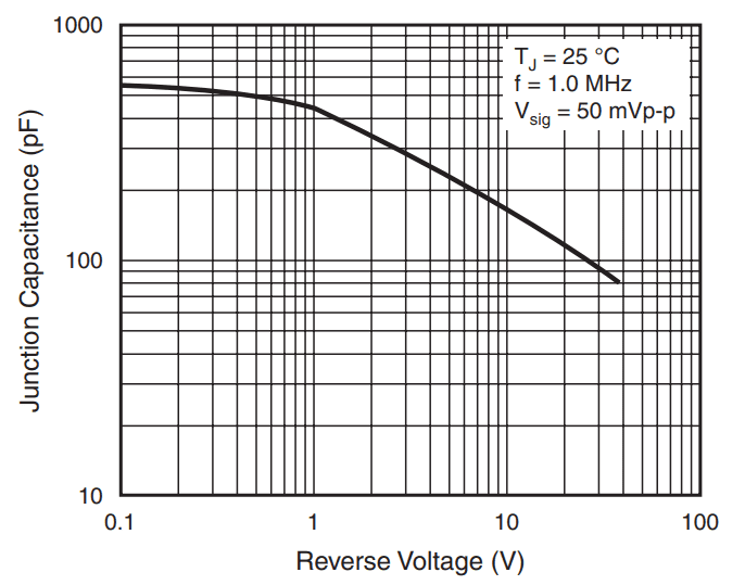

Example junction capacitance in reverse bias for the Vishay 1N5822-E3/54.
ESD Protection
Certain low-voltage or slower transient events can be reliably protected against with Schottky diodes. An example is shown in the circuit diagram below. In this example, two Schottky diodes are placed as pull-up elements to a power rail in reverse bias. The low voltage drop of these diodes enables clamping of moderate currents in reverse bias back to ground from moderately strong ESD events. A very similar application is used in motor control or when driving large inductive loads; placing the Schottky diode parallel around the load in reverse bias will create the same effect and will protect the driver circuit from damage should a back EMF surge event occur. Should very high levels of ESD protection be needed, a good option is something like a gas discharge tube.
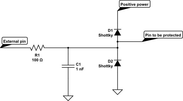

ESD protection with Schottky diodes.
When you need to find high power Schottky barrier rectifiers to use in your next design, use the complete set of search features in Ultra Librarian. The Ultra Librarian platform gives all users access to sourcing data, PCB footprints, ECAD/MCAD models, and a library of reference designs to help users speed up development. All ECAD data you’ll find on Ultra Librarian is compatible with popular ECAD applications and is verified by component manufacturers to help streamline your operations.
Working with Ultra Librarian sets up your team for success to ensure streamlined and error-free design, production, and sourcing. Register today for free.