Site icon Free Online PCB CAD Library

TPS54620 Datasheet: Analysis

View of TPS54620 package top and bottom.

View of TPS54620 package top and bottom.

The TPS54620 datasheet provides all critical information about device operation and details.

All devices need power to operate, but power delivery methods are vast and customizable. One method is a step-down buck converter that reduces the voltage from the power input to increase the current at the output. Whether the application is for high-density distributed power systems, high-performance point of load regulation, or communication infrastructure, the TPS54620 is an excellent choice. Before implementing it into your circuit, this short analysis of the TPS54620 datasheet will give designers an idea of what to expect from the device.

TPS54620 Datasheet Pinout
Name Number Type Description
RT / CLK 1 Input Selects between RT mode and CLK mode. An external timing resistor adjusts the device's switching frequency; in CLK mode, the device synchronizes to an external clock.
GND 2, 3 Ground Return for control circuitry and low-side power MOSFET.
PVIN 4, 5 Power Power input. Supplies the power switches of the converter.
VIN 6 Power Supplies the control circuitry of the power converter.
VSENSE 7 Input Inverting input of the gm error amplifier.
COMP 8 Output Error amplifier output, and input to the output switch current comparator. Connect frequency compensation to this pin.
SS/TR 9 Output Slow-start and tracking. An external capacitor connected to the pin sets the internal voltage reference rise time. The voltage on this pin overrides the internal reference for track and sequence.
EN 10 Input Enable pin. Float to enable. Adjust the input undervoltage lockout with two resistors.
PH 11, 12 Output Switch node.
BOOT 13 Input A bootstrap cap is necessary between BOOT and PH. The voltage on this cap carries the gate drive voltage for the high-side MOSFET.
PWRGD 14 Ground Power Good fault pin. Asserts low if the output voltage is low because of the thermal shutdown, dropout, overvoltage, EN shutdown, or during slow start.
Exposed Thermal Pad 15 Ground The thermal pad of the package and signal ground; it requires soldering for proper operation.

TPS54520 Datasheet Basics

The TPS54620 is a 17V, 1.6A synchronous step-down buck converter with two integrated n-channel MOSFETs in a quad-flat no-lead (QFN) package. The device supports switching frequencies from 200 to 1600 kHz. The on-chip circuit also features a phase-locked loop (PLL) control that synchronizes the switching cycle to the falling edge of an external clock. The default startup condition is when VIN is less than 4 V. The total operating current for the device when not switching and under no load is approximately 600 uA, with a quiescent current of 2 uA. Alternatively, the output can support currents up to 6A. 

There are several integrated functions of the component accessible by the pinout. An external capacitor supplies the bias voltage for the integrated high-side MOSFET between the BOOT and PH pins. An undervoltage lockout (UVLO) monitors the boot capacitor voltage; this action allows the PH pin to recharge the boot capacitor. The device can operate at a 100% duty cycle (full uptime) as long as the boot capacitor voltage exceeds the BOOT-PH UVLO threshold (typically 2.1 V). The device also has a power-good (PWRGD) comparator with hysteresis that monitors the output voltage through the VSENSE pin. The PWRGD pin connects to an open-drain MOSFET which outputs low whenever the VSENSE pin is >+/- 10% of the reference voltage or high whenever the VSENSE pin is < +/- 6% of the reference voltage. Finally, the SS/TR (slow start/tracking) pin minimizes inrush current on power up.

TPS54620 Features

Looking more in-depth, the TPS54620 has the following features:

  • Fixed-frequency pulse width modulation (PWM) control – The device uses an adjustable fixed-frequency peak current-mode control. The external resistors on VSENSE provide a comparison point for the output voltage to an internal voltage reference that drives the COMP pin. This error output converts to a current reference: when the power-switch current reaches the current reference, the high-side power switches off and the low-side power switches on.
  • Continuous Current Mode (CCM) Operation – As a synchronous buck converter, the device normally operates under CCM for all conditions.
  • VIN and Power VIN (PVIN) pins – The VIN pins power the control circuits, while PVIN supplies the input to the power converter system. Tied together, their input voltage can range from 4.5 to 17 V. Separately, VIN can range from 4.5 to 17 V, while PVIN can range from 1.6 to 17 V. 

Ultra Librarian Simplifies Design Variants

The TPS54620 datasheet gives designers many implementation options and ideas for devices centered around a step-down buck converter. Whether it’s the TPS54620, other similar devices, or completely different components, designers don’t want to spend precious design time creating footprints, simulation models, and schematic symbols. With Ultra Librarian, it’s fast and easy to get all your verified CAD models, as shown below for the TPS54620, and design data in one place. 

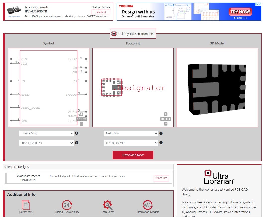
Schematic symbol, footprint, and 3D model for the TPS54620 from UL.

Working with Ultra Librarian sets up your team for success to ensure streamlined and error-free design, production, and sourcing. Register today for free

Exit mobile version