
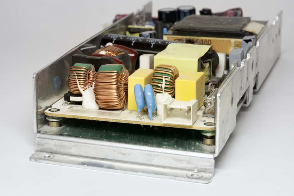
Synchronous buck converters are commonly used in switch-mode power supplies
The most important function of any electrical/electronic system is to ensure that power is accurately distributed to all necessary components and devices. Without meeting this basic requirement, no electrical product can operate reliably. For many electronic products, power is supplied via an external supply that may be linear or switch-mode.
The use of switch-mode power supplies (USPSs) typically require voltage step-up (boost) or step-down (buck) conversion. This voltage control and regulation can and is often accomplished with circuitry external to the power supply source. In order to develop power distribution circuits that satisfy the reliability and efficiency requirements for modern electronics, understanding the functionality and operation of synchronous buck converter design is necessary.
Buck Converter Types and Uses
Buck converters, which step down the voltage from a power supply source to match the level required for a load or loads, one of the most common energy operations for electronic systems. Common usage examples; include stepping down nominal 12 VDC power inputs to usable levels to drive internal circuit boards in personal computers and converting high voltage DC to a lower level for the various operational systems needed for electric vehicles (EVs). Basically, buck converters can be classified as one of three types, as listed below.
The range of utilization for buck converters can be seen by looking at a classification of DC-DC converters, as shown below.
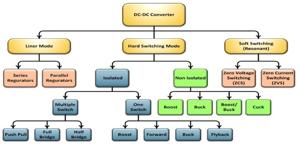
DC-DC converter classification. Image source.
As shown above, buck converters are used all types of DC to DC power switching applications. Prior to implementing a buck converter, it is necessary to clearly define your performance objectives. Doing so will help you decide whether to use the less complex and cost effective buck converter or synchronous buck converter design, which requires less components and space, and can be significantly more efficient.
Buck Converter Design Considerations
If efficiency or minimizing power loss are key design objectives for your power distribution, a synchronous converter is the better option. Prior to examining the considerations for a good synchronous buck converter design, it is informative to review the basic buck converter circuit operation. An example circuit is shown below.
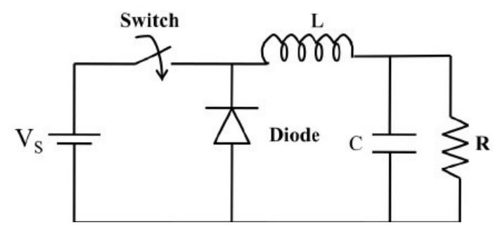
Basic buck converter circuit. Image source.
As shown above, the buck converter is a relatively simple electronic circuit that is comprised of common passive components–it is noteworthy, that some designs employ a transistor instead of a diode. The device gets its name from the fact that the voltage across the energy storage element, inductor L in the figure above, opposes or “bucks” the supply voltage, VS. This can be seen in the graph below.
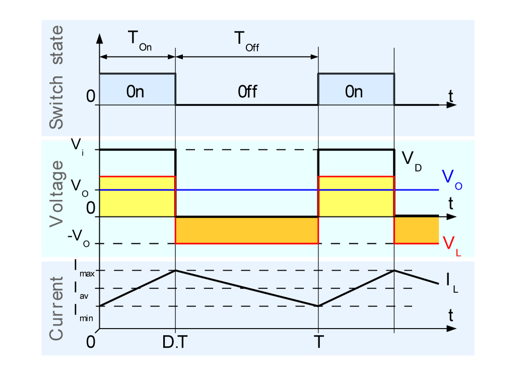
Buck converter operation graph. Image source.
As shown in the figure, during the ON state (switch is closed) the inductor current is increasing and the inductor voltage–which is opposite in polarity to the source voltage–causes a lower voltage potential across the load. When the switch is opened, the inductor voltage drop ensures the output voltage remains below the source level. As the inductor current decreases, a magnetic field is created that stores energy from the inductor. This stored energy becomes the source for the load during the OFF state (switch is open) and the forward-biased diode completes the circuit path.
Deriving a Synchronous Buck Converter
The basic buck converter has the advantages of simplicity; however, the use of a diode results in the power loss of Eq. (1).
Ploss = VD x (1-Duty Cycle) x Iout (1)
where VD is the voltage drop across the diode
DC is the duty cycle or the ratio of the ON state to the total period
Iout is the load current
This loss can be significantly reduced by replacing the diode with a second switch, which transforms the buck converter circuit into a synchronous buck converter design, as shown below.
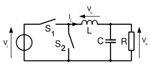
Synchronous buck converter design circuit. Image source.
The loss w.r.t. to the second switch in the synchronous buck converter circuit above is given by Eq. (2), below.
Ploss = VS2 x (1-Duty Cycle) x Iout (2)
and substituting for the switch voltage gives the loss equation for the synchronous buck converter.
Ploss = (Iout2 x R2) x (1-Duty Cycle) (3)
Typically, a transistor with low conduction resistance is selected. For example, a MOSFET with a low drain to source resistance, which significantly reduces power loss and contributes to improved efficiency with respect to the basic buck converter.
Creating the Best Synchronous Buck Converter Design
The choice of switches is important for a good synchronous buck converter design. However, there are additional guidelines, as listed below, that should be followed to realize the best design for your application.
By incorporating the guidelines above, along with good PCB layout practices, you can create a synchronous buck converter design that will meet or exceed your design objectives and aid in optimizing your board development process.
If you’re looking for CAD models for common components or important guidelines for creating the best synchronous buck converter design, Ultra Librarian helps by compiling all your sourcing and CAD information in one place.
Working with Ultra Librarian sets up your team for success to ensure streamlined and error-free design, production, and sourcing. Register today for free.


