Step 1: Requirements Definition and Component Selection
Begin DDR4 reference design development by establishing clear performance targets, environmental requirements, and cost constraints. Define data rate requirements, capacity needs, and operating temperature ranges. Select memory controller and DRAM devices based on application requirements, ensuring compatibility between controller capabilities and memory specifications.
Component selection significantly impacts routing complexity and signal integrity performance. Choose memory devices with consistent electrical characteristics and proven reliability records. Consider package options carefully, as smaller BGA packages offer better high-frequency performance but increase assembly complexity and cost.
Step 2: Schematic Symbol and Footprint Verification
Accurate schematic symbols and PCB footprints form the foundation of successful DDR4 reference designs. Utilize manufacturer-vetted CAD models from trusted sources like Ultra Librarian to ensure dimensional accuracy and pin assignment correctness. Verify that schematic symbols include all necessary power, ground, and signal connections with proper pin numbering.
Ultra Librarian’s comprehensive database provides verified symbols, footprints, and 3D models for major memory manufacturers, including Samsung, Micron, SK Hynix, and controller providers like Intel, AMD, and Qualcomm. These manufacturer-approved models include accurate mechanical dimensions, thermal characteristics, and electrical parameters essential for successful implementation.
Step 3: PCB Stackup and Layer Planning
Design PCB stackups specifically optimized for DDR4 signal characteristics and power delivery requirements. Typical DDR4 implementations require 6-8 layer stackups to provide adequate signal layers, dedicated power planes, and proper return path management. Plan layer assignments with data signals routed on stripline layers when possible to minimize crosstalk and EMI emissions.
Maintain consistent dielectric thickness and material properties throughout the stackup to ensure impedance control. Use low-loss dielectric materials (Df < 0.004 at 1GHz) for high-speed signal layers to minimize insertion loss at DDR4 frequencies. Plan via structures carefully, utilizing HDI technology where PCB miniaturization and/or trace density demands require smaller via sizes.
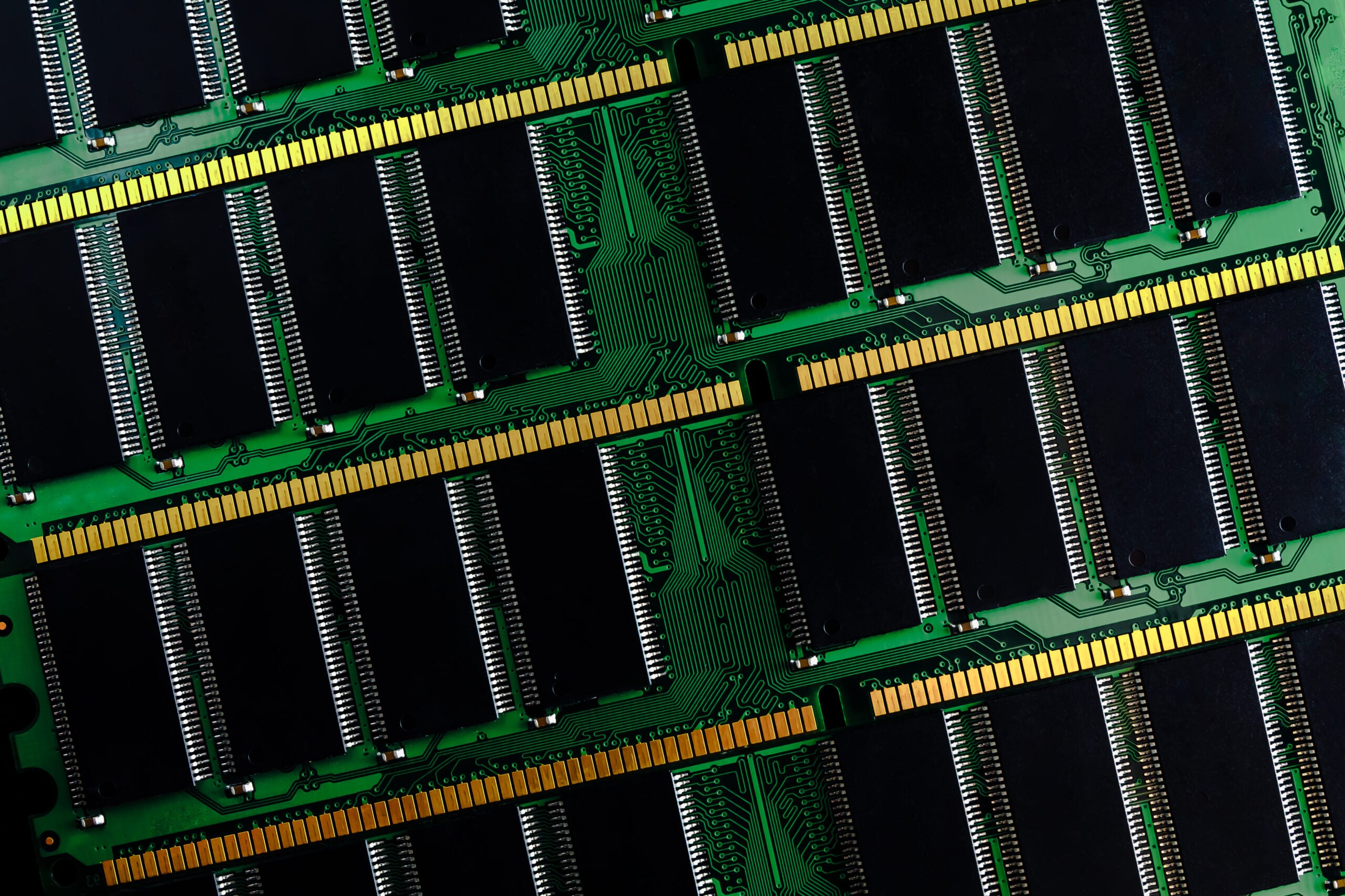
Step 4: Component Placement Optimization
Strategic component placement drives DDR4 routing success and signal integrity performance. Position memory devices in order of their daisy-chain sequence, minimizing trace length differences between devices. Maintain consistent spacing between memory packages to enable uniform routing patterns and simplify length matching requirements.
Place decoupling capacitors as close as possible to memory device power pins, with high-frequency ceramics positioned within 5mm of the target pins. Plan power delivery component placement to minimize loop inductances and provide clean, stable power to all memory devices throughout the operating frequency range.
Step 5: High-Speed Routing Implementation
Execute DDR4 routing using advanced PCB design tools capable of managing complex timing constraints and signal integrity requirements. Route data byte lanes as matched groups, maintaining consistent impedance and minimizing crosstalk through proper spacing and layer assignments. Implement fly-by topology for address/command/control signals, maintaining daisy-chain connections in numerical device order.
Apply differential routing techniques for clock signals, maintaining tight coupling and consistent 100Ω differential impedance throughout the signal path. Use via optimization strategies to minimize discontinuities at layer transitions, implementing techniques like via stitching for reference plane connections.
Optimization Strategies for DDR4 Reference Designs
Although implementing DDR4 technology has inherent advantages, you must follow the guidelines listed below to optimize your DDR4 reference design.
DDR4 Reference Design Optimization Guidelines- Implement comprehensive pre-layout simulation using IBIS models to verify timing margins and identify potential signal integrity issues before physical implementation
- Optimize via structures by using HDI technology with smaller drill sizes (0.1-0.15mm) to minimize stub length and reduce signal discontinuities at high frequencies
- Apply advanced power delivery techniques, including power plane segmentation, dedicated VTT regulation, and strategic decoupling capacitor placement for optimal PDN performance
- Utilize manufacturer-verified CAD models from Ultra Librarian to ensure accurate footprints, symbols, and 3D models that prevent costly design iterations and manufacturing issues
- Implement robust EMI mitigation through proper ground plane design, signal return path management, and strategic component placement to minimize electromagnetic emissions
- Plan for manufacturing tolerances by including design margins that accommodate PCB fabrication variations, component placement accuracy, and assembly process capabilities
- Incorporate comprehensive test points and debug features to enable thorough validation and troubleshooting during prototype development and production testing
- Design for thermal management considering memory device heat dissipation, ambient temperature effects, and thermal cycling impacts on signal integrity and reliability
- Validate designs through simulation using advanced signal integrity and power integrity analysis tools before committing to prototype fabrication
- Document design decisions thoroughly, including constraint files, routing guidelines, and assembly requirements to ensure consistent implementation across design revisions
|
Successful DDR4 reference design development requires systematic attention to signal integrity, power delivery, component selection, and manufacturing considerations. By following the guidelines above and utilizing manufacturer-verified CAD models, you can optimize your DDR4 reference design to meet performance targets while maintaining cost-effectiveness and reliability.
If you’re looking for CAD models for common components or the best DDR4 reference design guidelines, Ultra Librarian helps by compiling all your sourcing and CAD information in one place.
Working with Ultra Librarian sets up your team for success to ensure streamlined and error-free design, production, and sourcing. Register today for free.