


TI PMP23193 SMPS reference design from UL
Switching mode power supplies (SMPSs) are commonly implemented as the key element of PCB power distribution networks (PDNs). These power supplies have major advantages, as compared to linear power supplies, that include:
Advantages of SMPS vs Linear Power Supply✅Higher efficiency ✅Greater power density ✅More compact design ✅Less heat generation ✅Greater range of input voltage |
Switching mode power supply (SMPS) design has become increasingly complex as engineers demand higher efficiency, smaller form factors, and enhanced reliability in modern electronic systems. The SMPS reference design is an attractive solution for creating an SMPS design from scratch. These reference designs provide a proven foundation for AC/DC power conversion, offering standardized approaches that reduce development time while ensuring optimal performance. These validated designs are essential starting points for creating robust power supply solutions across industrial, automotive, and consumer applications.
Understanding AC/DC SMPS Reference Design Fundamentals
Reference designs eliminate the guesswork in component selection, PCB layout optimization, and regulatory compliance, providing engineers with tested configurations that meet stringent performance requirements. SMPS reference designs provide specific benefits, including:
Key Benefits Of Using SMPS Reference Designs
|
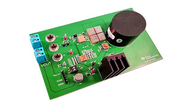
These benefits are exhibited in the TI PMP23193 reference design of a synchronous buck converter below.

TI PMP23193 SMPS reference design of synchronous buck converter from UL
To fully leverage the advantages of an SMPS reference design, it is important to emphasize the following essentials:
Important Considerations of SMPS Reference Design
SMPS reference designs often employ transformers to adjust power levels to an appropriate level for implementation in the intended circuit and/or system. Therefore, power factor correction and input stage, as well as secondary side regulation and control, are important design considerations.
Power Factor Correction and Input Stage Design
Modern AC/DC SMPS reference designs incorporate sophisticated front-end circuits that ensure compliance with power quality regulations while maximizing energy efficiency. The input stage typically includes EMI filtering, bridge rectification, and PFC circuitry that conditions the incoming AC power for downstream conversion stages. Reference designs provide proven filter component values, layout guidelines, and grounding strategies that minimize electromagnetic interference while maintaining high efficiency across the full AC input range of 85-265VAC.
Secondary Side Regulation and Control Architecture
Advanced SMPS reference designs implement primary side regulation (PSR) techniques that eliminate the need for optocouplers and secondary feedback circuits. This approach simplifies the overall circuit topology while maintaining excellent load and line regulation. The controller incorporates constant voltage/constant current (CV/CC) operation with built-in protection features including output overvoltage, overcurrent, and short-circuit protection.
How to Optimize Your SMPS Reference Design
Creating an SMPS reference design implementation that best meets your design requirements can be daunting. However, by following the guidelines below, you can achieve an implementation optimized for your project.
Guidelines for SMPS Reference Design Optimization
|
The benefits of reference design implementation extend beyond individual projects, enabling organizations to develop consistent design methodologies, reduce development risks, and accelerate time-to-market for new products. As power supply requirements continue to evolve toward better efficiency, greater power, and enhanced reliability, reference designs provide the foundation for accomplishing these goals while maintaining design control and predictability.
SMPS reference designs represent proven pathways to successful AC/DC power supply development, offering significant advantages in development time, design reliability, and performance enhancements. However, it is important to rely on proven SMPS tools and resources.
If you’re looking for CAD models of common components or design information to optimize your SMPS reference design, Ultra Librarian compiles all your sourcing and CAD information in one place.
Working with Ultra Librarian sets up your team for success to ensure streamlined and error-free design, production, and sourcing. Register today for free.