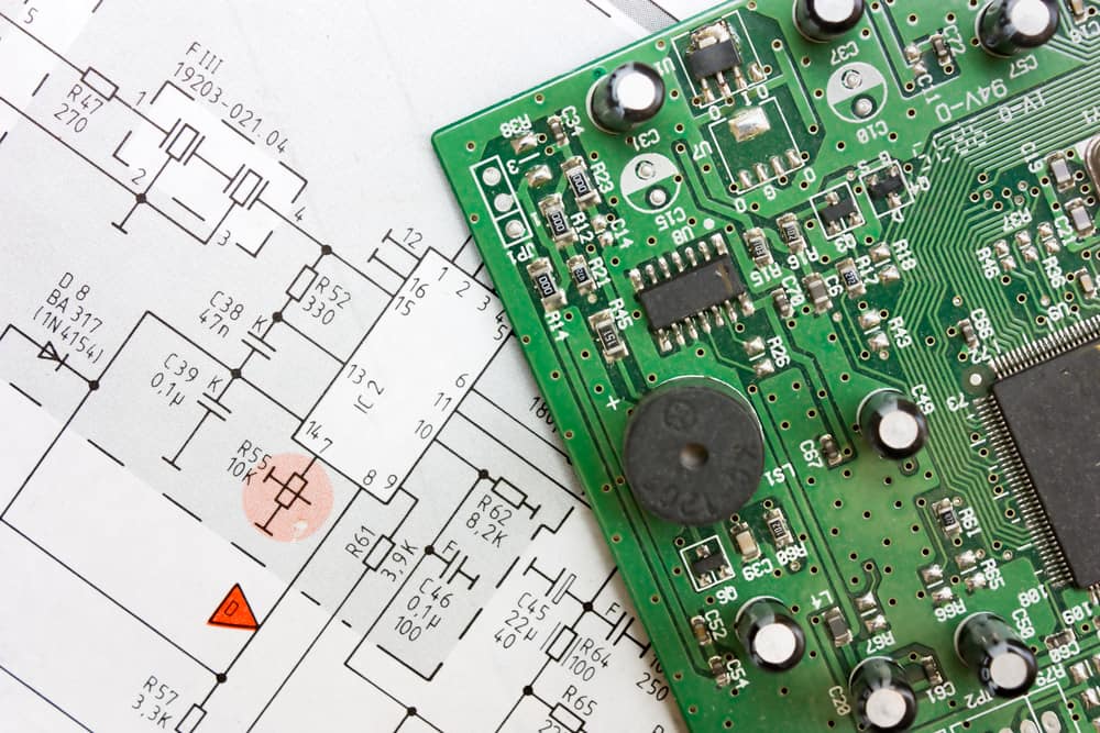
PCB diagram and circuit board
I have heard it said–more than once–that engineers are bad at following directions. Common examples cited to support this observation are that engineers never read assembly instructions and will never, under any circumstances, stop and ask for driving directions. If there is any truth to these claims, it certainly does not apply to the designing of electronic circuit boards. In fact, the reliance upon diagrams is foundational to PCBA design.
The ability to read and create PCB diagrams of various degrees of complexity is essential to all phases of board development. However, understanding circuit boards requires knowledge of PCB diagram types and how they relate and are used for the corresponding board.
What Constitutes a Circuit Board?
An electronic circuit board can be quite complex. This is evidenced by the number of manufacturing processes, included those listed below, required to create an assembled PCBA.
Major Processes to Build a Circuit Board
Fabrication Processes
- Board imaging
- Inner layer and surface etching
- Arranging, stacking, and pressing the board layers
- Drilling holes for vias and mounting
- Plating vias
- Applying solder masking, silk screen, and finishing
Assembly Processes
- Applying solder paste
- Picking and placing components
- Initial soldering
- Rework (if necessary)
- Final soldering
- Cleaning
- Depanelization
The above processes are typical of all automated PCBA manufacturing operations, whether for prototyping or full production. In certain cases, additional actions are necessary–for example, when rigid-flex or full-flex boards are being built. The final board assembly consists of the following elements:
- Components
- Connectors
- Drill holes–plated through holes (PTHs) and non-plated through holes (NPTHs)
- Copper traces
- Copper planes–for signal routing and ground connections
- Insulation layers–to separate copper planes
- Protection coating–solder mask and conformal coating (optional)
This list, although not exhaustive, is representative of the elements for most circuit boards. Many board designs place a premium on size, which translates into a dense surface topology that is very difficult–if not impossible–to follow, which is one reason why PCB diagrams are essential.
How to Read PCB a Diagram
As indicated above, one of the most significant reasons for PCB diagrams is to make the circuits they represent easier to understand. This benefit is utilized by different personnel and for different purposes throughout the process chain of circuit board development and production. Additionally, PCB diagrams are used by end-users to better understand circuit board operations and functionality. Common types of PCB diagrams and how they are used are listed below.
| USES AND APPLICATIONS OF PCB DIAGRAMS | |||
| PCB Diagram Type | Primary User | Information | Application |
| Schematic | PCB Designer | Shows all component symbols and the netlist that connects them. | To create the original design and make subsequent design changes. |
| PCB Layout | Contract Manufacturer (CM) | Shows the footprints for components, trace locations and dimensions, layer stackup, silkscreen markings, etc. | Used by the CM to fabricate and assemble the physical board. |
| Drill Hole Diagram | Contract Manufacturer (CM) | Shows the location and dimensions for PTHs and NPTHs. | For drill hole placement during fabrication. |
| Block Diagram | End-User | Shows the major elements of the board. | Operational and functionality overview. |
As the table above indicates, PCB diagrams are important to everyone involved with the building and use of the circuit board. However, the diagrams must be used properly.
Using Diagrams to Understand Circuit Boards
Unless you are the creator of the circuit board design, gaining detailed insight into the design’s intent, including performance objectives, can be elusive and excruciatingly time-consuming. However, by following a few simple guidelines, you can mitigate these issues and quickly uncover the design’s purpose.
Key Guidelines to Understanding Circuit Boards
🔑 Clearly define the information you are seeking.
🔑 Choose the PCB diagram type most likely to provide the information desired.
🔑 Know common symbols and correct PCB terminology for your diagram.
🔑 Isolate sub-circuits, traces, and/or components for evaluation.
🔑 Use supplementary information such as component datasheets.
🔑 Make use of analysis techniques and tools.
By following the guidelines above, you should be able to determine the purpose of most circuit boards. Many times, understanding a circuit board from a macro perspective is sufficient. However, at other times, a more refined or component-level understanding is required. In these cases, you will need to use component diagrams, such as the schematic symbol, PCB layout footprint, and CAD model for a popular component, shown below.
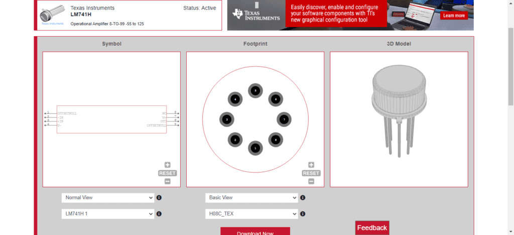
Component diagrams for the LM741 operational amplifier
The combination of using PCB diagrams and component diagrams effectively should enable you to gain whatever depth of understanding of circuit boards you require.
If you’re looking for CAD models for common components or depth in understanding circuit boards, Ultra Librarian helps by compiling all your sourcing and CAD information in one place.
Working with Ultra Librarian sets up your team for success to ensure streamlined and error-free design, production, and sourcing. Register today for free.


")