It isn’t so long ago that I was working through school and taking apart remotes and radios in my house to learn about different electronics. Now that I’m working in the industry, it’s easy to take for granted what is being given to me through industrial organization and standards. It never fails to rain on my day, though, when I get component information or footprints that simply haven’t been organized or documented properly.
Finding free PCB footprints and schematic symbols online is rarely difficult; there are a host of options out there, and some even with verifiable partnerships with distributors and manufacturers. It’s knowing where to find these accurate and reliable sources of data that becomes the trick.
What are PCB Footprints?
A PCB footprint is a pattern used to create the physical form of an electronic component. These footprints, which are also called land patterns, contain precise dimensional measurements vital to the assembly of a final PCB part. Importantly, though, land patterns and outlines do not always equate. Land patterns give the size of the pads, whereas outlines give the size of the body and may or may not include pad information. Errors in these measurements can cause soldering problems, spacing issues, current flow difficulties, or fit mismatches. PCB footprints are measured to the nearest hundredth, thousandth, or sometimes ten-thousandth, of an inch.
Their resultant parts can only be created with specialized tools with the ability to shave off tiny dimensions of material for precision. There are a wide variety of footprints available and different manufacturers have their own PCB footprint standards. The IPC is an international standards body for the electronics community that attempts to standardize electronics design, and many companies either follow the IPC’s standards directly or create standards compatible with IPC regulations. A good way to check the quality of a PCB footprint is to compare its properties to IPC standards. They have been supporting the electronics industry since 1957.
What are Schematic Symbols?
A PCB schematic is an illustration of the current and layout in an electronic circuit. Designers should create a schematic before handling a PCB footprint. A single PCB schematic can be translated into many PCB footprints. Starting with the footprint could lead to unexpected problems in electrical conductivity when designers try to shoehorn circuits into the right places without enough room or stability.
Most schematic symbols represent components, but symbols also exist for other useful features of PCB design. These symbols can include test points, mounting holes, or ground rails. As with PCB footprints, schematic symbols are standardized by an international organization.
This organization, called the International Electrotechnical Commission (IEC), was founded in 1906. Its database of schematic symbols covers components, conductors, binary logic elements, and many other pieces of electrical hardware. Additionally, there is the organization of IEEE (ANSI) or the Institute of Electrical and Electronics Engineers (American National Standards Institute) which has very recognizable languaging. These schematic symbols are essential for correctly diagramming a circuit, showing the direction of current, and depicting the devices connected by those circuits.
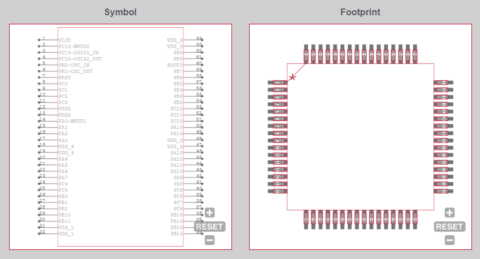
Schematic symbol and footprint of STMicroelectronics STM32L151RDT6 MCU.
Where can Designers Find Free PCB Footprints or Schematic Symbols?
The most reliable places to find guidelines for standardizing the creation of PCB footprints or schematic symbols are directly from the IPC and IEC. Since those footprints and symbols are part of established standards, designers can be completely confident those footprints and symbols will be understood by any engineer with the appropriate knowledge. The IPC and IEC provide information free of charge and include information to help engineers learn any symbols or packaging in standards they do not yet know.
If you’re not using the IPC or IEC databases, it is particularly important for designers to find high-quality PCB footprint and schematic symbol information. This information is often found in libraries, which may be easier to go through than the full IPC and IEC standards. Designers should double-check their libraries for accuracy whenever possible. Standards can change and the PCB industry is currently in a period of rapid evolution. The Institute of Electrical and Electronics Engineers (IEEE) is a reliable place to both validate PCB libraries and to look for more information on specific footprints and symbols.
Finding reliable PCB footprints and schematic symbols is more important than ever since a new generation of electronics professionals is getting information from the Internet. Finding proper technical information is essential and if engineers know where to look, they can get versions of many different electronics and engineering standards. Engineers rely on standards as their source of truth, so a reputable source of PCB footprints or schematic symbols should be easy to validate against those standards.
Ultra Librarian validates its libraries against multiple electronics standards and strives to provide designers with the highest quality CAD software. We also have partnerships with many reputable electronics vendors, including Texas Instruments, Maxim, Toshiba, and TE Connectivity.
Ultra Librarian is committed to making the PCB design process easier for everyone. Register today to get all the benefits of reliable PCB software that takes the busy work out of creating complex designs. Register today for free!


")