

Modern FPGAs, systems-on-chip (SoCs), and AI processors demand high current at low voltages, putting pressure on point-of-load (PoL) regulators. Board space is strictly limited, and thermal management rules are non-negotiable when current spikes from, for example, AI workloads can go from milliamps to several amps in nanoseconds. The TDK FS1003-0600 Reference Design provides a proven hardware solution to such constraints. It is built around TDK’s µPOL (micro Point-of-Load) technology, integrating the pulse-width modulation (PWM) controller, power MOSFETs (or power switches), and inductor into a single compact integrated circuit (IC) package.
This article details the specifications, layout rules, and integration tactics for this highly integrated DC-DC converter platform, helping you supply clean power to complex digital loads without wasting board space.
Evaluating the TDK FS1003-0600 Reference Design
The TDK FS1003-0600 Reference Design is an evaluation board for the FS1406 series of micro-Point-of-Load (µPOL) DC-DC converters. The converters are ultra-compact, highly integrated power modules that combine the controller, power switches, and inductor into a single package to deliver regulated low-voltage power close to the load. The primary purpose of the TDK FS1003-0600 is to demonstrate how the FS1406 module family achieves high output current in an extremely small footprint, using a design verified by TDK’s own power engineering team.
In a traditional PoL layout, a discrete PWM controller, a high-side field-effect transistor (FET), a low-side FET, and an external inductor are required for DC-DC power conversion and voltage regulation. Each of these components occupies its own printed circuit board (PCB) footprint. More critically, the traces routing current between them introduce parasitic inductance that degrades switching efficiency, generates ringing, and contributes to electromagnetic interference (EMI).
To address this, TDK packages the controller, power switches, and inductor into one compact module (measuring 3.3mm x 3.3mm x 1.5mm). The reference board supplies up to 3A of continuous output current from a 12V input with minimal external components. You only need to add input and output capacitors to complete the circuit.
PoL Comparison: Discrete vs. Integrated Module
| Feature | Discrete PoL Converter | TDK µPOL (FS1406 Series) |
| Component Count | High (Controller, 2x FETs, Inductor, Passives) | Low (Module + I/O Capacitors) |
| PCB Footprint | Large (> 50mm sq) | Very Small (~11mm sq) |
| Parasitic Inductance | Variable, highly dependent on designer layout | Minimized internally by the manufacturer |
| Control Loop | Analog (requires external compensation network) | Digital (internally compensated) |
| Output Voltage | Fixed or via an external resistor divider | Dynamic via PMBus/I²C command interface |
| Thermal Dissipation | Spread across multiple packages | Centralized at the module thermal pad |
TDK FS1003-0600 in Practice: Powering AI Accelerators and Edge Computing
Modern AI accelerators and high-performance field-programmable gate arrays (FPGAs) place very strict demands on their power delivery networks, requiring compact converters that can respond quickly to sudden changes in load current while fitting close to the processor core.
When an AI processing core activates, the current draw spikes from milliamps to several amps in nanoseconds. This steep di/dt causes the supply voltage to sag. If the voltage drops below the processor’s minimum threshold (a margin of only 50–100 mV on a 0.85 V core rail), the device resets or corrupts data.
Keeping the rail stable under these conditions requires either an extremely fast control-loop bandwidth, a large bank of low equivalent series inductance (ESL) output capacitance, or both. Integrated point-of-load solutions like the TDK FS1003-0600 address these constraints directly, combining tight regulation and compact footprint in a single module.
Edge Computing and Battery-Powered Applications
Edge inference shifts the power delivery problem in a different direction. As AI workloads move out of centralized data centers and into autonomous sensors, robotic controllers, and ruggedized industrial gateways, the power delivery network must contend not just with peak performance demands but also with the strict energy budgets of battery operation. These systems frequently transition between idle states and active inference bursts.
To manage these rapid operating-mode changes, efficient power delivery becomes just as important as compute capability. The FS1406 modules support a PMBus/I²C (power management bus) command interface that allows the host processor to adjust the output voltage setpoint dynamically during operation. When the processor drops into a low-power sleep state, it can command the regulator to reduce the core voltage, thereby substantially reducing static and dynamic power dissipation. When a high-priority inference task is queued, the processor restores the nominal core voltage before the compute burst begins. This active voltage-scaling capability is built into the module: no external digital-to-analog converter (DAC), additional controller, or resistor-switching network is required.
Industrial and Safety-Critical Designs
Industrial applications introduce environmental stressors that compound the electrical challenges: wide ambient temperature ranges, vibration, humidity, and variable input voltages from distributed 12 V or 24 V bus rails. To achieve this, the µPOL integration strategy helps reduce the number of discrete components and solder joints. Fewer discrete components means fewer potential mechanical failure points in vibration-prone environments.
The thermal via array mandated by the reference layout (described below) ensures that the module’s junction temperature remains within rated limits even in elevated-ambient industrial enclosures. The small, dense footprint also simplifies conformal coating and potting workflows, both of which are common in industrial and automotive-adjacent designs.
PCB Layout Guidance and Implementation Tips
The schematic is only half the design. If you fail to follow the physical layout in the reference files, the power supply will overheat or generate excessive electromagnetic interference (EMI).
TDK FS1003-0600 Layout Tips
| PCB Design | Placement Rule | Engineering Impact |
| Input Capacitors (VIN / PGND) | Place high-frequency ceramic capacitors as close as possible to VIN and PGND pins. Further, minimize trace length and via count; use multiple wide parallel vias when layer transitions are necessary. | Every extra millimeter of trace increases switching loop inductance, which raises EMI radiation and worsens switch-node ringing. Therefore, long or narrow return paths increase noise and instability. |
| Output Capacitors (VOUT) | Mount capacitors close to VOUT pins and keep traces short and wide. | Output capacitors provide the instantaneous current required during load transients. However, additional trace inductance slows their response, increasing voltage undershoot and degrading transient performance. |
| Ground Plane | Use a continuous, uninterrupted ground plane directly beneath the module. Avoid routing signals through power return paths. | Fragmented return currents couple switching noise into sensitive circuitry, degrading analog-to-digital converter (ADC) accuracy and causing false triggering in high-speed digital interfaces. |
| Thermal Vias | Place a dense via array under the exposed thermal pad. Use specified via size, pitch, and count from the reference design. | Transfers heat into internal copper planes acting as a distributed heatsink. Insufficient via density increases junction temperature, reducing efficiency and risking thermal shutdown. |
| Switching Node (SW) | Keep SW trace extremely short with minimal copper area. Avoid sharp corners and keep away from sensitive/analog routing layers. | The SW node has high di/dt switching between VIN and GND. Therefore, large loops act as antennas, increasing EMI and noise coupling into nearby circuits. |
The Value of Pre-Verified Power Designs
Building a power supply from scratch introduces significant project risk. Engineers must ensure control-loop stability, select inductors that will not saturate under peak loads, and accurately predict thermal performance under worst-case operating conditions. Because these factors are tightly interconnected, a design that appears correct at the component level can still develop unexpected system-level stability issues.
Therefore, a verified reference design reduces these risks by pre-validating control-loop compensation, component selection, and thermal performance across the full operating range. By directly copying manufacturer-provided component values and copper geometry, the power delivery network is kept within known safe electrical and thermal limits, reducing engineering time and avoiding costly PCB re-spins caused by instability, overheating, or EMI issues that typically add weeks of delay.
This approach also scales across product families and multi-rail systems: once a design is validated using a reference layout (e.g., within the FS1406 family), the same capacitor ratios, layout rules, and thermal via patterns can be reused across additional rails in FPGA or SoC power architectures, compounding engineering efficiency across the full design.
Start Your Design with Verified CAD Models
Designing reliable power delivery for high-performance silicon requires physical precision. By utilizing the TDK FS1003-0600 reference design alongside verified component data, you prevent footprint errors and ensure your PCB handles the required current density.
Ultra Librarian provides PCB designers with the exact schematic symbols, PCB footprints, and 3D STEP models required to place these TDK power modules into your layout correctly the first time. Register today for free and download the exact CAD assets you need to bring your hardware to market faster.

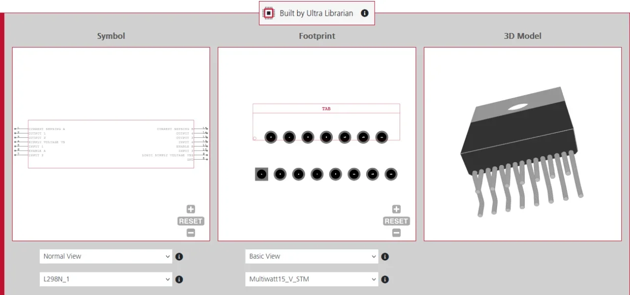
 If you’re looking for any of our component footprints or models, we have readily available and free options for you and your design team. Search our library for the solution you’ve been looking for.