Run out of GPIO pins? Turn to the 74HC595 datasheet to solve that problem with a single 16-pin IC. PCB designers frequently use this shift register to expand microcontroller outputs to drive LED matrices, operate multi-digit 7-segment displays, or manage relay banks.
Built on silicon-gate C2MOS technology, the 74HC595 delivers low power consumption, high noise immunity, and stable operation, making it well-suited for space-constrained designs, such as densely populated custom display boards or compact IoT control modules. You feed it data over three microcontroller lines and get eight independent digital outputs in return.
Understanding the specific timing requirements and electrical limits in our datasheet guide ensures these eight outputs behave exactly as intended.
74HC595 Pinout and Internal Architecture
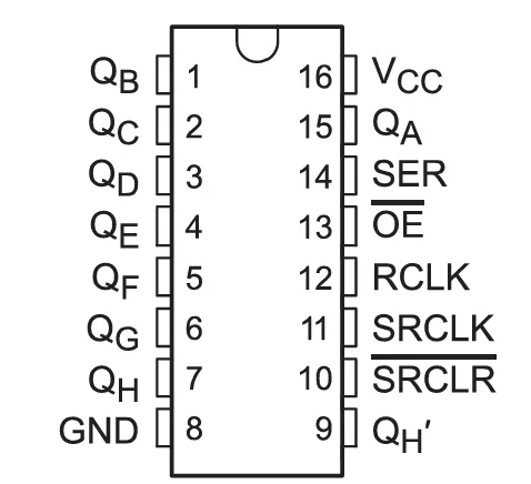
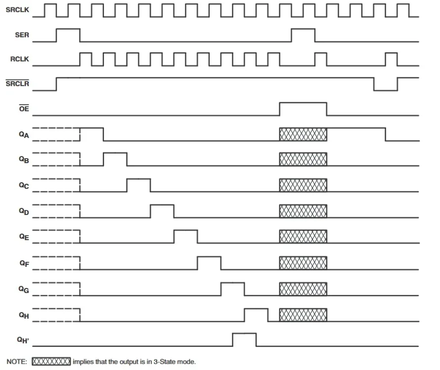
The 74HC595 is an 8-bit serial-in, parallel-out (SIPO) shift register with an 8-bit storage register, featuring a serial data input, eight parallel data outputs (Q0–Q7), and a serial output for cascading. To prevent outputs from fluctuating while new bits stream in, the internal architecture physically separates data acquisition from the final output stage. More specifically, data shifts into an internal register bit by bit, then transfers to an output storage register only when you pulse the latch clock.
Because both the shift register clock (SRCLK) and storage register clock (RCLK) are positive-edge-triggered, correctly timing these independent pulses determines exactly when the outputs update. Knowing each pin’s role is the foundation for correct wiring and firmware development, and can be easily found in the 74HC595 datasheet.
Pin Assignments
- Q0–Q7 (Pins 15, 1–7): The eight parallel data output pins.
- GND (Pin 8) / VCC (Pin 16): Power supply connections.
- Q7S / QH’ (Pin 9): Serial data output, used exclusively for daisy-chaining multiple shift registers.
- MR / SRCLR (Pin 10): Master Reset (active-low). Pulling this pin low clears the internal shift register. Tie it to VCC during normal operation.
- SHCP / SRCLK (Pin 11): Shift Register Clock. Data on the serial input pin shifts into the register on the rising edge of this signal.
- STCP / RCLK (Pin 12): Storage Register Clock (Latch). The rising edge moves data from the shift register to the parallel output pins.
- OE (Pin 13): Output Enable (active-low). Tie to GND to enable outputs; pulling it high places all outputs into a high-impedance state.
- DS / SER (Pin 14): Serial Data Input. Your microcontroller feeds the bitstream here.
Key Specifications from the 74HC595 Datasheet
The specifications below define hard operational limits. Exceeding these values guarantees erratic behavior or permanent damage to the silicon. Treat them as constraints to design around, not margins to push.
74HC595 Datasheet: Electrical Characteristics
| Parameter | Specification | Notes |
| Operating Voltage (VCC) | 2.0V to 6.0V | Compatible with both 3.3V and 5V logic |
| Max Clock Frequency | 55 MHz (at 5V) | Well above typical LED/display refresh rates |
| Typical Output Drive (Per Pin) | ±6 mA | Recommended continuous operating current |
| Absolute Max Output Current (Per Pin) | 35 mA | Damage threshold; do not use as design target |
| Max Total Current (VCC/GND) | 70 mA | Hard package limit when all outputs are active |
| Quiescent Current (ICC) | 80 µA (max) | Suitable for battery-operated circuits |
Notably, the 74HC595 datasheet specifies a typical output drive of ±6 mA per pin. While the absolute maximum rating is 35 mA per output, running the chip at that level continuously can stress the IC and shorten its lifespan. To maintain reliable long-term operation, the 74HC595 is best used for low-current tasks, such as driving LEDs through current-limiting resistors.
The total package current limit is the constraint most engineers miss. Specifically, the standard 74HC595 has a strict thermal limit of approximately 70mA total for the entire chip. This cumulative limit creeps up on you quickly. If you try to drive eight LEDs at 20 mA each, the chip will overheat. That is 160mA through the package at worst-case load, more than double what the IC can handle. Always calculate the worst-case current with all outputs active simultaneously.
Practical Applications and Microcontroller Interfacing for 74HC595 Datasheet
LED Driving and 7-Segment Display Control
Driving LED arrays and 7-segment displays is the most common use case for the 74HC595 shift register. A standard 7-segment display needs eight independent control lines for the seven segments plus the decimal point. That means a single 74HC595 maps directly onto that requirement.
When connecting LEDs directly to the outputs, size your current-limiting resistors so that each LED draws no more than 6 mA under worst-case conditions, keeping total package current within the 70 mA limit. Then, for higher loads such as LED strips, motors, or relays, pair the 74HC595 outputs with external drivers such as transistors or MOSFETs. For example, a Darlington array, such as the ULN2003, works well, as the shift register handles logic-level switching while the array handles the current.
Cascading Multiple 74HC595 Registers for Expanded Output Control
Multiple 74HC595 shift register ICs can be daisy-chained to control 16, 32, or virtually any number of digital outputs without using additional microcontroller pins. The wiring is straightforward:
- Connect QH’ (Pin 9) of the first 74HC595 to SER (Pin 14) of the second.
- Tie all SRCLK (clock) pins together to the same microcontroller clock pin, and tie all RCLK (latch) pins together to the same microcontroller latch pin.
- The first 8 bits you send will overflow from the first chip’s QH’ pin and slide directly into the second chip’s SER pin. To update all 16 (or more) outputs simultaneously, shift out all the necessary bytes for every chip in the chain, then pulse the shared latch pin high. This updates all outputs simultaneously without any visible flickering.
Note that signal integrity and timing start to degrade after chaining many chips, especially at higher clock speeds. For this reason, add decoupling capacitors and verify setup/hold timing margins when cascading more than three or four devices.
Bit-Banging vs. Hardware SPI for Shift Register Interfacing
You have two options for clocking data into the 74HC595: software bit-banging or hardware serial peripheral interface (SPI).
- Software bit-banging, such as Arduino‘s shiftOut() function, manually toggles GPIO pins to generate clock and data signals. It works for basic indicator LEDs but consumes CPU cycles proportional to the bit count.
- Hardware SPI offloads the repetitive work of generating clock pulses and shifting individual bits to a dedicated peripheral. At 5V, the 74HC595 device can handle a maximum clock frequency of around 55 MHz; hardware SPI can operate well within such a range while freeing the CPU entirely. Connect the SPI MOSI pin to DS (Pin 14), SPI SCK to SRCLK (Pin 11), and use a standard GPIO pin for the RCLK latch. The result is faster refresh rates and no visible flicker in multiplexed LED matrices.
Each VCC pin should have a bypass capacitor to prevent power disturbances; 0.1 µF is recommended for a single-supply configuration. Place it as close to Pin 16 as the PCB layout allows.
Find Verified 74HC595 CAD Models and Components
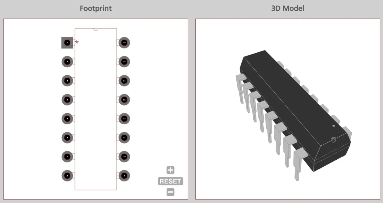
After reviewing the capabilities in the 74HC595 datasheet, make sure to use accurate CAD models to implement this shift register on your board. Working with Ultra Librarian gives your team instant access to verified footprints and 3D models, all formatted for popular ECAD applications. You can also track down pricing and inventory from worldwide distributors directly through Ultra Librarian, so register today for free.
Working with Ultra Librarian sets your team up for success by ensuring streamlined, error-free design, production, and sourcing. Register today for free.

 If you’re looking for any of our component footprints or models, we have readily available and free options for you and your design team. Search our library for the solution you’ve been looking for.