Heat is the silent killer of electronics. As devices shrink and power densities rise, managing thermal performance is a fundamental requirement for reliability. If you ignore it, you risk catastrophic failure. Engineers often reference the Arrhenius equation to explain this effect. In simple terms, higher temperatures speed up material degradation processes such as electromigration, dielectric breakdown, and solder fatigue. A common rule of thumb derived from this model is that for many failure mechanisms, every 10 °C increase in operating temperature roughly doubles the failure rate.
This advanced tutorial on PCB thermal management techniques focuses on high-power designs where standard practices often fall short:
- The physics of heat generation and thermal pathways in PCBs
- Strategic layout techniques for high-power designs
- Thermal interface materials and active cooling methods
- Design standards, simulation tools, and verification strategies
The Physics of Heat in PCBs
Before discussing PCB thermal management techniques, let’s talk about where heat comes from. Heat in a printed circuit board (PCB) travels via three mechanisms:
- Conduction,
- Convection
- Radiation
In most designs, conduction is your primary concern, followed closely by convection.
Heat Sources
Joule heating, the conversion of electrical energy into heat as current flows through a resistive material, is the most common culprit. In PCBs, current flowing through traces and components generates heat due to resistance (I2R). High-speed switching devices like MOSFETs, IGBTs, and processors also generate significant thermal energy during state changes.Joule heating, the conversion of electrical energy into heat as current flows through a resistive material, is the most common culprit. In PCBs, current flowing through traces and components generates heat due to resistance (I2R). High-speed switching devices like MOSFETs, IGBTs, and processors also generate significant thermal energy during state changes.
The Thermal Path
Your goal is to create a low-resistance path for heat to escape from the junction (the hot internal part of the chip) into the ambient environment.
- Junction-to-case: Heat moves from the silicon die to the component package.
- Case to PCB/Heatsink: Heat transfers through solder joints or thermal interface materials (TIMs).
- PCB to Ambient: The board itself acts as a heat spreader, releasing energy into the air via natural or forced convection.
Strategic Layout Techniques
The most effective thermal management starts at the layout stage. No amount of fans can fix a fundamentally poor board design.
Copper Weight and Planes
Copper is an excellent thermal conductor. Increasing the copper weight from the standard 1 oz (35 µm) to 2 oz or 3 oz improves the board’s ability to spread heat laterally.
For high-power designs, you should maximize the coverage of ground and power planes. These large copper pours act as heat spreaders. Connecting multiple internal ground planes with stitching vias creates a massive thermal mass that pulls heat away from localized hotspots.
Component Placement
Avoid grouping high-power components. While it might simplify routing to keep all your power regulators in one corner, this creates a thermal hotspot that is difficult to cool. Spread these components across the board to utilize the full surface area for dissipation.
Also, be mindful of temperature-sensitive components. Placing electrolytic capacitors or crystal oscillators next to a hot Voltage Regulator Module (VRM) will degrade their performance and shorten their lifespan.
Thermal Vias
Thermal vias are plated through-holes designed to transfer heat from the top layer component to the inner layers or the bottom side of the board. They are arguably the most cost-effective cooling tool.
Design Guidelines for Thermal Vias:
- Placement: Place vias directly inside the thermal pad of surface-mount components (active pads) or as close as possible.
- Size: A diameter of 0.3mm (12 mil) is typically ideal. It offers a good balance between drill cost and thermal capability.
- Pitch: Space vias about 1.0mm to 1.2mm apart in a grid pattern.
- Plating: Ensure a minimum plating thickness of 25µm to guarantee adequate thermal conductivity.
Cooling Methods and Interface Materials
When layout alone isn’t enough, you need external help.
Heatsinks and Enclosures
Heatsinks increase the surface area available for convection. They are typically made of aluminum (cheap, light) or copper (heavy, expensive, better performance). For extreme power, the enclosure itself can act as a heatsink. You can machine bosses into an aluminum chassis that contacts the hot components directly.
Thermal Interface Materials (TIMs)
Microscopic air gaps exist between any two mating surfaces. Since air is a terrible thermal conductor (0.026 W/m·K), these gaps block heat transfer. TIMs fill these voids.
Comparison of Common TIMs
| TIM Type | Thermal Conductivity (W/m·K) | Best Use Case | Pros | Cons |
| Thermal Grease | 3.0 – 8.0+ | CPUs, high-power GPUs | Excellent performance; fills microscopic voids well. | Messy; can pump out over time (dry out). |
| Thermal Pads | 1.0 – 5.0 | VRMs, Memory chips | Easy to apply; fills large gaps; electrically insulating. | Lower performance than grease; requires compression. |
| Phase Change | 3.0 – 5.0 | Production heatsinks | Solid at room temp, liquid at operating temp. Consistent. | Requires a specific temperature to activate. |
| Gap Fillers | 1.0 – 4.0 | Uneven surfaces | Dispensed like liquid; cures to a soft solid. Low stress. | Expensive dispensing equipment is needed. |
Design Standards and Simulation
Relying on “rules of thumb” is risky for high-power boards. You need quantitative thermal data to ensure trace temperatures remain within safe limits, copper weights are correctly specified, temperature rise stays below component derating thresholds, and long-term reliability targets (e.g., MTBF) are met. Thermal design decisions should be based on validated current-carrying capacity models, material properties, and simulation results.
IPC Standards
Two main standards guide thermal design:
- IPC-2221: The generic standard for PCB design. It provides basic charts for trace width vs. current, but its thermal data is outdated and conservative. It can be used for quick early-stage estimates or low-power designs where precision is not critical.
- IPC-2152: Standard for Determining Current-Carrying Capacity in Printed Board Design. This is the physics-based standard you should use. It accounts for thermal conductivity, board stackup, and internal vs. external layers more accurately. It should be used for high-power, high-current, or reliability-critical designs. This should be your primary reference for trace sizing and thermal validation.
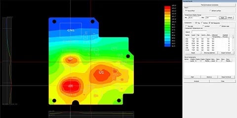
Simulation Tools
Simulation allows you to see the invisible. Computational Fluid Dynamics (CFD) tools can predict airflow, temperature gradients, and hotspots before you fabricate a single board.
- CFD Tools: Ansys Icepak, Mentor Graphics FloTHERM, and Cadence Celsius are industry heavyweights.
- Specialized Analysis: Altair PollEx offers dedicated single PCB thermal analysis for rapid verification, while Altair SimLab is ideal for complex system-level thermal analysis involving enclosures and airflow.
- Process: Import your ECAD data (ODB++ or IPC-2581), define component power dissipation, and set boundary conditions (ambient temp, airflow).
- Benefit: You might discover that a tall capacitor is blocking airflow to a critical MOSFET, a problem you would never spot on a 2D layout screen.
Practical PCB Thermal Management Techniques
- Remove the Solder Mask: For high-current traces, expose the copper by removing the solder mask. You can then add extra solder during assembly to artificially increase the trace thickness.
- Use the Chassis: If your board is mounted in a metal box, use thermal pillars or thick thermal pads to bridge the gap between the PCB ground plane and the chassis.
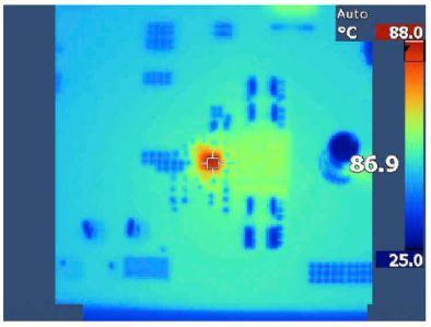
- Verify with Thermal Cameras: Simulation is great, but reality is better. Use a FLIR camera during the prototype phase to validate your thermal model.
Effective PCB thermal management techniques are not just about slapping a heatsink on a hot chip. It requires a holistic approach and starts with the right components. Ultra Librarian provides the CAD models you need, compatible with popular ECAD applications and sourced from worldwide distributors.
Working with Ultra Librarian sets your team up for success, ensuring streamlined and error-free design, production, and sourcing. Register today for free.