


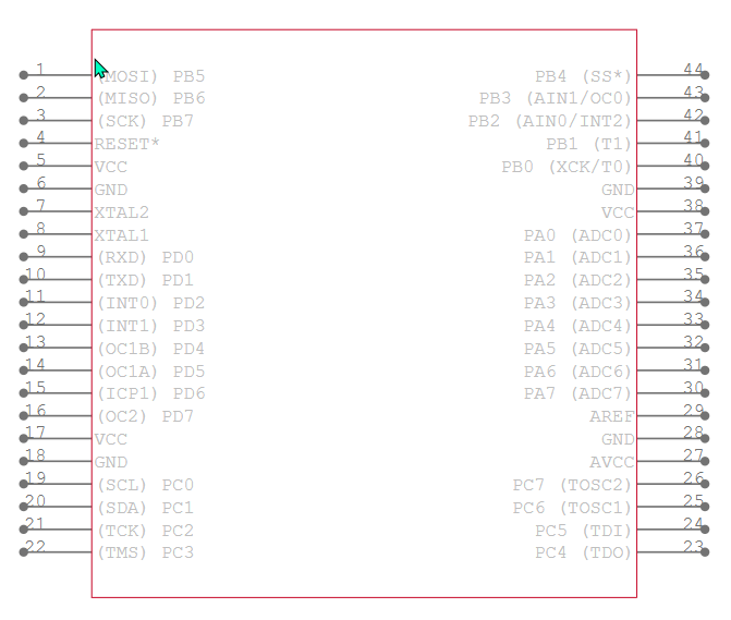
A schematic symbol for the 44-pin ATMEGA32A-AU integrated circuit
Virtually all circuit boards begin as a PCB layout diagram that was generated from a schematic. As the foundation for your layout, it is critical that your schematic convey required data and information about the board components, accurately. The schematic symbol library serves this purpose.
When building the schematic symbols for your component library, it is important to know and follow best practices. This is especially true with schematic symbols for integrated circuits, where parametric specifications, such as pin arrangement, are critical for manufacturing and successful operation. By understanding symbol elements and the standards that guide their creation, you can most effectively design your schematic and help facilitate efficient PCB design and development.
Schematic Symbols for Integrated Circuits: Naming & Reference Designators
Integrated circuits (ICs) are depicted in schematics as rectangular blocks featuring labeled pins that are arranged in the schematic symbol as shown below.
Learning to interpret and draw schematic symbols for integrated circuits is a key part of understanding electronics, and any Electronic Components Guide. Each IC symbol serves as a bridge between the physical chip and its schematic representation, capturing the logical flow of power, data, and control signals.
For single-package ICs, pin 1 typically starts at the top-left corner of the package and continues counterclockwise around the body—this mirrors both physical package orientation (e.g., DIP, QFP, BGA) and schematic convention. On the symbol itself, pin numbers are clearly labeled alongside functional names (e.g., VCC, GND, CLK), allowing designers to correlate the schematic with the chip’s datasheet. Generally, schematic symbols for integrated circuits are represented as follows.
Typical Schematic Symbol for IC Representation
- A rectangular box represents the IC’s body, with pin names and numbers alongside each connection.
- Pins are often arranged by function: Inputs left, outputs right, power top, ground bottom, consistent with schematic readability guidelines.
- ICs are typically labeled with a reference designator starting with U or IC (e.g., U1, U2, U3).
- Inside the box, each pin is named according to datasheet functions—e.g. VCC, GND, CLK, CS—with alternate names optionally added.
This representation is not all-inclusive for all ICs; however, it does illustrate a general pattern for symbol pin organization adhered to by many IC manufacturers. As an example, the ATMEGA 32A AU schematic symbol, shown below along with the corresponding footprint and 3D CAD model below, illustrates typical local pin arrangement, grouped functional blocks, and special pin designations.
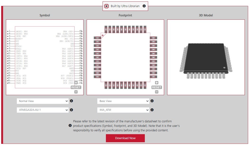

ATMEGA32A-AU CAD Models from UL
Logical Pin Arrangement
The IC is drawn as a rectangular block with pins labeled by both signal name (e.g., MOSI, RESET, GND) and port name (e.g., PB5, PD0). This dual-labeling makes it easy to map pins to both the hardware function and the datasheet naming convention.
- Inputs like MOSI, RESET, and XTAL1 appear on the left side.
- Outputs and general-purpose I/O (e.g., PB0, PA7, PC6) are typically on the right side.
- Power pins (VCC, GND, AVCC, AREF) are placed at the top and bottom, aligning with schematic best practices for power distribution flow.
Grouped Functional Blocks
The symbol groups pins by function, which improves readability:
- Port B (PBx) and SPI pins (a common communication protocol standard) are at the top left/right.
- Port D (PDx) in the middle left handles UART (another common communication protocol standard) and interrupts.
- Port A (PAx) on the right is used for analog-to-digital (ADC) channels.
- Port C (PCx) at the bottom handles I2C (SCL, SDA), TWI, and JTAG.
Special Pins and Symbols
- Pins like RESET*, TDI, TDO, and AREF have special purposes (reset, debug, reference voltage), often marked with asterisks or alternate names in parentheses.
- XTAL1 and XTAL2 indicate crystal oscillator connections, a common inclusion in microcontroller symbols.
Large Multi-Pin ICs
A giant block of 100+ pins for schematic symbols for integrated circuits is overwhelming. Designers who deal with the schematic need quick access to the signals relevant to their task—power, digital I/O, analog, etc. Splitting these into separate blocks keeps each view focused .
- Logical organization: Functional units like MCU_Core, MCU_IO, MCU_PWR, or MCU_Analog naturally map to signal groups. This mirrors the chip’s internal structure and helps engineers mentally “reconstruct” the IC from schematic to silicon. Place POWER and GROUND units on a power-sheet; CORE on the main; I/O blocks near their respective circuits. Use sheet labels/net labels to tie them together logically.
- Support for multi-sheet schematics: Large designs often span multiple pages. Grouping related pins by sheet (e.g., power on sheet 2, I/O on sheet 3) prevents line crossing and keeps each page uncluttered.
- Optional “Full Symbol” Block: Some libraries include a main symbol (U5) with all pins, plus smaller modules (U5A, U5B). This retains pin visibility while offering focused placement where needed.
Multi-Pin IC Example
In some cases, particularly microprocessors (MPUs) and microcontrollers (MCUs), a single pin may be used for several types of signals as indicated below.