SCHEMATIC SYMBOLS


Your confidence in the accuracy of the Ultra Librarian CAD libraries is extremely important to us. As a result, all models are rigorously vetted before introduction into the library. To help ensure consistency across models we have chosen to utilize globally recognized industry standards from IPC and ASNI wherever possible. This not only helps ensure a common set of rules for library creation but also provides common naming conventions and guidelines that can be used by you and your downstream design and manufacturing partners.
On top of our standards-based process, our build methodology utilizes a single database structure. The data is stored in a vendor-neutral format. This means that it stores all the relevant data from all the various CAD tools that we support, preventing any inconsistencies across CAD types. The majority of the patterns in the library are built using the Ultra Librarian desktop software to assist in consistency and reliability. Where appropriate, components are based on the IPC-7351B standard. Exceptions would include thru-hole components as well as parts built to a specific standard and so labeled. Where possible components have been built using the 3-tiered complexity level of; least material condition, nominal material condition, and maximum material condition.
Symbols and Footprints are built in English units (mils) unless otherwise specified. Metric units are entered when appropriate (such as the pitch of metric pin spacing) but all dimensions are shown in inches rounded to three decimal places and rounded to the nearest Mil. Metric numbers are rounded to two decimal places. Actual locations are stored internally to 8 decimal place accuracy. Users can switch between metric and English units.
Each footprint has the assembly outline of the part to the max condition. The silkscreen outline is 5 mils larger than the outline of the part on each side. The pins and the Z height are located on the appropriate assembly layer for the CAD tool.
Each pattern contains a silkscreen of the component on the appropriate silkscreen layer. It avoids crossing pads where possible but depends on a silkscreen removal routine to completely remove silkscreen from pads.
SCHEMATIC SYMBOLS
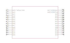
Microchip, PIC16F18055-I/SO
PCB FOOTPRINTS

Mitel, MH89790BN40
Each component has a RefDes attribute on the silkscreen layer of the pattern. In applicable tools, there is also a RefDes2 attribute or second RefDes attribute on the top assembly layer. Where possible a maximum and minimum height attribute has been added to each footprint. Each footprint has dimensions on a separate layer to identify key features of the footprint. Each footprint has both a silkscreen layer which clearly identifies the part and any orientation. There is an assembly layer containing data representing the exact size of the part. Footprints contain a placement boundary if this information is available in the targeted CAD tool. It contains test probe boundaries that change size based on the z-axis or height of the footprint. Data is contained for each footprint in our internal database to provide a 3-D DXF formatted footprint if desired.
Each pattern has a pick and place point for assembly installed. It is placed on pin one of the pattern for thru-hole components and the centroid of the component for SMT patterns. Each SMT component contains a glue dot as its centroid (where applicable). Components contain a placement point for referencing the pickup point in the CAD tool. This point will reference the 0,0 location of the component for the CAD Tool. Each component contains a rectangle of drawn lines or a filled polygon (depending on the CAD tool) that designates the total size of the component and a rectangle defining its nominal size for use with the height attribute.
Each component has a RefDes attribute on the silkscreen layer of the pattern. In applicable tools, there is also a RefDes2 attribute on the top assembly layer. All RefDes attributes are centered in the middle of the part with a center-center justification. A 50 mil height attribute has been assigned to each component.
Each pattern contains a silkscreen of the component on the top silkscreen layer. It avoids crossing pads where possible but depends on a silkscreen removal routine to completely remove silkscreen from pads. Assembly information is included on the top assembly layer. It is intended to have a complete description of the component available on the silkscreen layer. Assembly information reflects the true size of the part. Silkscreen and assembly draw widths are 6 mils wide. All text is 50 mils high with a 5 mil stroke width. Pin one is identified on all polarized components.
3D STEP MODELS
All the 3D models in our library are built to the STEP-file format, ISO 10303-21. Since the 3D models are dynamically created from footprint information, the rotation, origin, and pins are going to be the same as the original footprint – no need to mate the two. Our 3D models are shape-based and export to .STL and STEP formats most accurately. All our 3D models are only able to be created from footprints that are built using our template system, which means about 85% of footprints are covered by 3D models.
Metric components have padstacks named per the IPC-7351B. By default, our components are built and delivered using English units and follow a naming convention that is similar, but not identical to the IPC-7351B.
Padstack Naming Conventions:
When appropriate, components contain local fiducials.
The naming of padstacks starts with a shape designator as follows:
R=Rectangular
O=Oval
E=Eliptical
D=Diamond
RD=Rounded Diamond
C=Circular
P=Polygonal

Motorola, MC68HC05F12FU80
Shape designator are followed by an “x” with the size in mils and then a y dimension with the size in mils. Example: RX40Y30 indicating a rectangular pad with a 40 mil x and a 30 mil y side. Size is followed by a drill size. SMT pads are designated as “D0.” Others as “D” followed by the drill size in mils. So the above example would expand to “RX40Y30D20″.
If this padstack is a blind via or buried via it is indicated by a suffix number.
If the padstack is modified from a standard or existing padstack it is designated with a suffix number.