
PCB Design Development: Guide
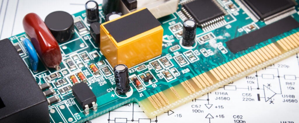
Results of a successful PCB design development process PCB design development, which includes schematic generation and PCB layout design, is a complex engineering process that demands precision, efficiency, and access to comprehensive component libraries. Success hinges on seamless schematic capture, accurate circuit connectivity, and having the right parts data at your fingertips when design decisions […]
How to Improve PCB Design for a Better Layout

How to Improve PCB Design Techniques is a crucial question to ask in the search for better product design Printed Circuit Board (PCB) design layout can make or break your electronic product’s performance, reliability, and cost-effectiveness. Even experienced engineers face challenges with signal integrity, thermal management, and component placement that can lead to costly redesigns […]
How to use UltraBOM
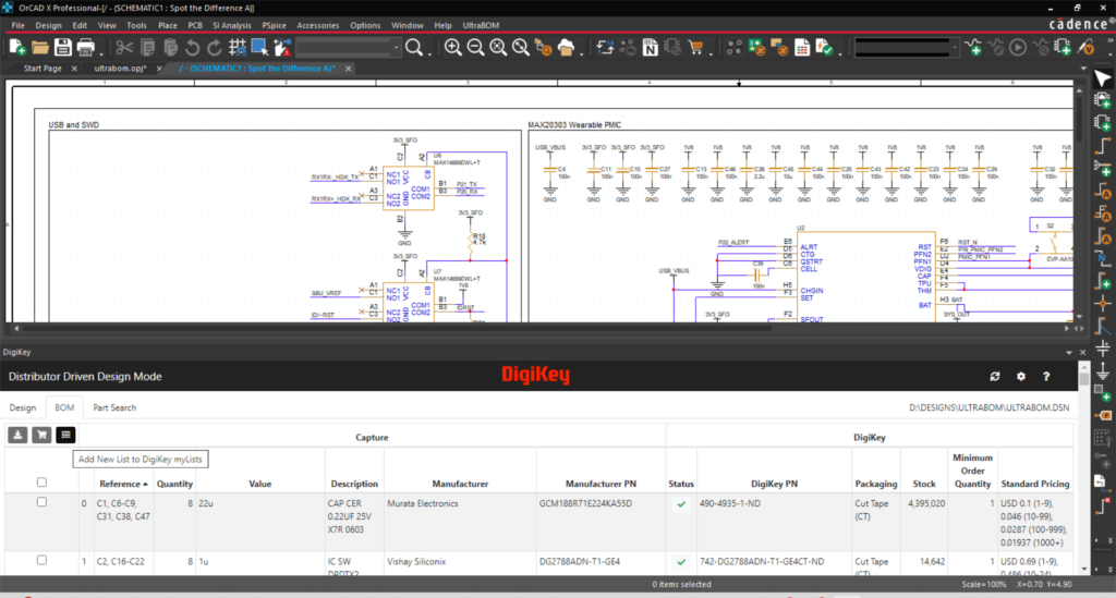
Example of how to use UltraBOM in OrCAD X Finding the right components is the first step in designing and developing your circuit board. It is also the most critical. Choosing the wrong components can result in unacceptable performance in the field, the inability to have your board built, or even failed procurement. Consequently, effective […]
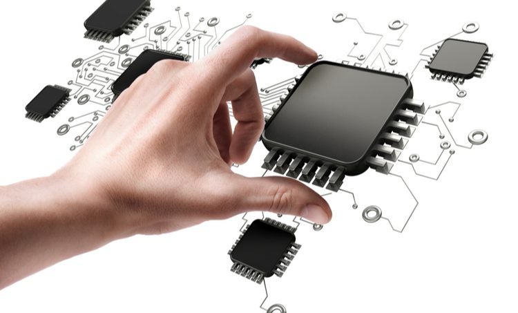
AI Electronic Circuit Design in 2025

An engineer reacting to an AI electronic circuit design for a complex problem in 2025 The question of when effective AI tools for PCB design would arrive has been answered. The future is now. In fact, with generative AI tools like ChatGPT, you can talk through your board design. Amazing, yes! The expansion of capabilities […]
High Current PCB Design Guidelines
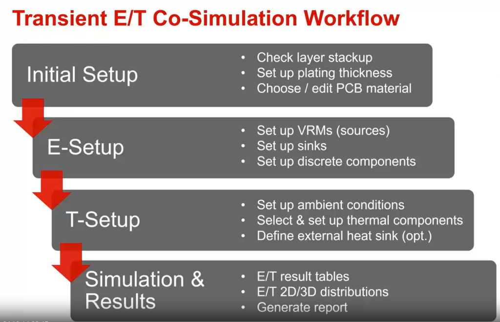
Transient electrical/thermal co-simulation workflow for high current PCB power design Designing printed circuit boards (PCBs) with high power PCB design guidelines presents unique challenges in both electrical performance and thermal management. In a recent webinar hosted by STMicroelectronics and EMA Design Automation, experts walked through their collaborative flow for optimizing a three-phase inverter reference board […]
PCB Antenna Footprint: What to Know

This piece will discuss footprints available around ‘antenna’ and also discussing RF and these types of components. We can also showcase some of your top partners as images for examples.
Schematic Gate Symbols: Explained

Schematic gate symbols allow engineers to visualize and efficiently design circuits that implement digital logic. As products, appliances, and systems get smarter, the electronics that drive them become more digital. PCBs are typically classified based on construction or application. Nevertheless, circuit boards that utilize digital components are predominant for board types like embedded systems containing […]
PCB Layout Bridge Rectifier: Important Design Guidelines

Cell phone chargers are one of the most common uses of electronic rectifiers. Some may say that love, money, or even coffee make the world go around. Engineers usually lean toward a more scientific answer, such as ‘power makes the world go around.’ There is a strong case for this perspective. Can you imagine what […]
ECAD Libraries/Models for Data-driven Design Workflows
Effective management of ECAD libraries/models is essential for efficient PCB design workflow. When downloading a new component, it is important to ensure strict organization of my component library in order to keep track of my ECAD models. There’s nothing more annoying than being unable to find a component model or design data in my library […]
Electronic Components Semiconductors: Guide
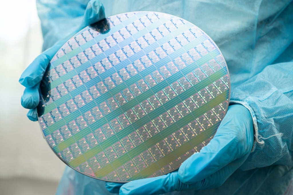
Electronic component semiconductor silicon wafer It is indisputable that the invention of the transistor opened the door for the current technological revolution. Today, it is becoming increasingly difficult to find products that do not leverage electronics to enhance capabilities and functionality. More often than not, these products and systems are driven by circuit boards that […]