
PCB Footprint Guidelines: Best Practices

A robust electronic components sourcing database enhances design efficiency, minimizes risks, and accelerates time-to-market for electronic products.
Essential CAD Design Library Guidelines
A robust electronic components sourcing database enhances design efficiency, minimizes risks, and accelerates time-to-market for electronic products.
PCB Footprint Creation: Basics For Your Next Design

Follow these PCB component footprint basics if you need to create symbols and footprints for your new circuit board CAD drawing.
PCB Component Placement Tolerance
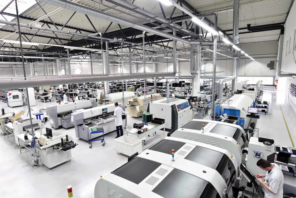
PCB component placement tolerance is a function of IPC footprint tolerancing and various stages of board processing accuracy. PCBs always have to do more with less. Miniaturization of electronics is a welcome development for consumer devices, but comes with additional complications for the designers and manufacturers. The product development team must optimally determine the best […]
Best CAD Library of 2026: Models, Files, and Designs

The best CAD library of 2026 models enables advanced analyses like thermal simulation Engineering and design professionals use CAD (Computer-Aided Design) libraries to reliably create 2D and 3D models and designs. Electronic component models can be assembled for analyses like thermal simulation and to enable efficient ECAD-MCAD integration. These libraries save time, reduce errors, and […]
Top Electronic Component Distributors
Knowing the top electronic component distributors helps you make the best selection for your PCBA development.
SMD LED Footprint: Characteristics and Layout
The SMD LED footprint is well-suited for a wide range of applications requiring compact and reliable lighting solutions.
Footprint Dimensions: Explained
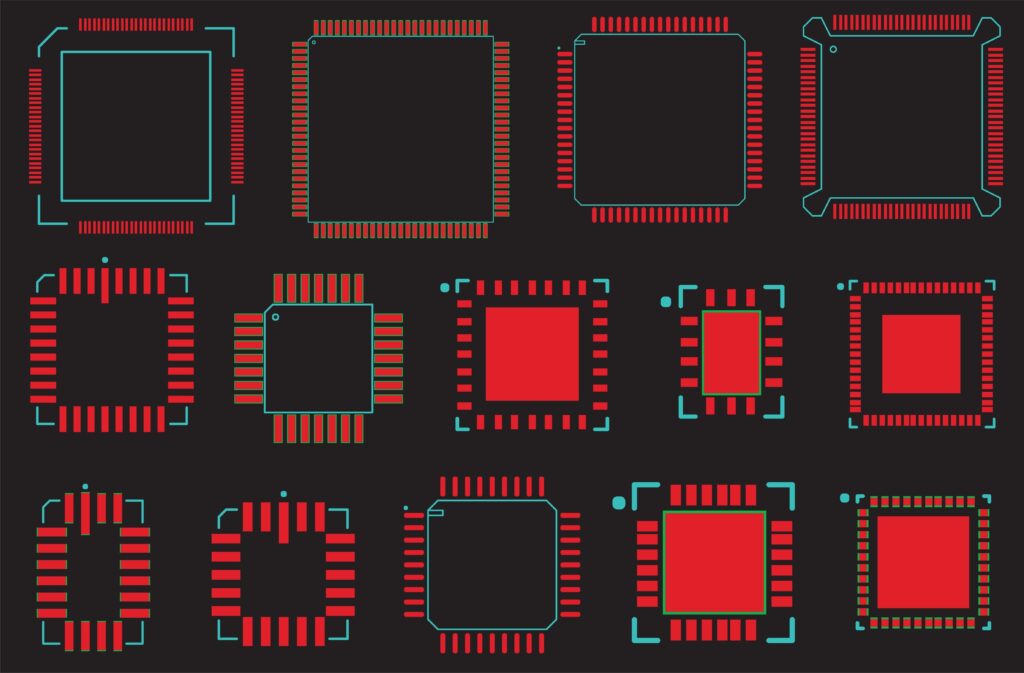
Understanding the importance of footprint dimension accuracy begins with knowing the difference between footprints and landing patterns.
PCB Library Creation: A Guide
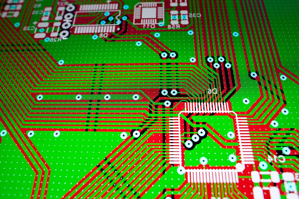
If you want to save time before you design your new board, follow these PCB footprint creation guidelines.
12 Basic Electronic Symbols and Their Functions
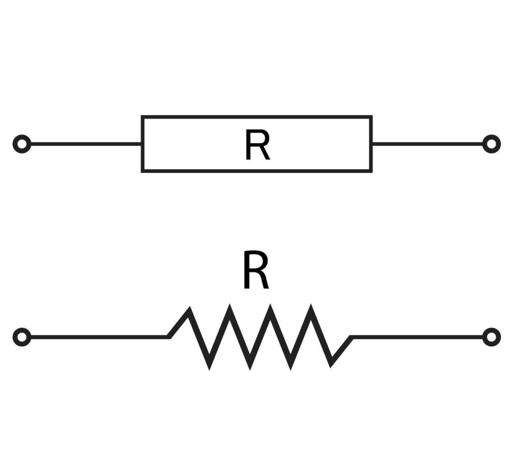
Good PCBA design begins with a clear understanding of basic electronic symbols and their functions—read on to learn more.