A BJT can be easily used for switching applications of a small load. But when you try to control a big load, the transistor starts to heat up due to the high energy loss involved in the emitter-collector path. In this regard, MOSFETs are ideal to improve circuit efficiency. The 2N7002 is one of the most widely used N-channel MOSFETs that offers low on-state resistance for low-current applications such as small servo motors. It utilizes a Double-Diffused MOS (DMOS) structure to offer high commutation speed and good efficiency at low voltage levels. The MOSFET also offers a fast switching speed and excellent thermal stability. Therefore, it is used in motor controls, converters, amplifiers, and drivers.
A thorough understanding of the 2N7002 datasheet and readily available CAD design data is required to make the best use of this MOSFET.
2N7002 Features and Pin Layout
Unique Features
The unique features of the 2N7002 MOSFET are:
- Low threshold voltage
- High breakdown voltage
- High input impedance
- Low input capacitance
- Fast switching speed
Pin Layout
The pin layout has been shown below.
Three pins of an N-channel MOSFET are equivalent to three BJT pins as follows.
| MOSFET | BJT |
| Gate | Base |
| Drain | Collector |
| Source | Emitter |
However, while BJTs are current-controlled devices, MOSFETs are voltage-controlled devices. Unlike BJTs, MOSFETs do not require gate current to operate. Instead, they require a minimum gate voltage, also known as threshold voltage, to switch to the ON state.
Understanding 2N7002 Datasheet
Absolute Maximum Ratings
The following table shows the absolute maximum ratings of the MOSFET.
| Symbol | Parameters | Value | Unit |
| VDSS | Drain to source voltage | 60 | V |
| VDGR | Drain Gate Voltage | 60 | V |
| VGSS | Gate to Source Voltage – Non-repetitive | ±20 | V |
| VGSS | Gate to Source voltage – continuous | ±40 | V |
| ID | Maximum drain current – continuous | 115 | mA |
| ID | Maximum drain current – pulsed | 800 | mA |
| PD | Maximum power dissipation derated above 25ºC | 200 | mW |
| Ttsg | Operating and storage temperature range | –55°C to +150°C | ºC |
| TL | Maximum lead temperature for soldering purpose | 300 | ºC |
As you can see, the MOSFET has been designed for low voltage and low current application. Operating the device beyond these limits may cause permanent damage to the internal circuit.
Electrical Characteristics
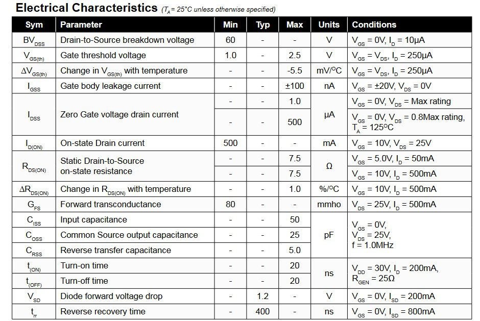
For the 2N7002, the typical VGS(threshold) value is 2.1 Volt, with a min-max window of 1 V to 2.5 V. This is so because the threshold voltage varies depending upon the operating temperature. The breakdown value VGS(breakdown) is ±20 V.
As per the 2N7002 datasheet, the transistor requires a minimum 1 volt at the gate to start conducting 250μA current. It can typically conduct 600 mA drain current at the standard gate to source voltage of 5V.
Also, the transistor can successfully drive a small load of 500 mA (ID) while maintaining a lowest drain-source voltage possible (VDS=0.6 volt).
The Transistor can achieve this at a maximum 10 volt VGS and a moderate resistance of 1.2 between the drain and the source RDS (on). That’s why, it has a very low power dissipation (PD) of around 200 mW.
The typical input capacitance (Ciss) is 20 pF. This capacitance value is much less than other MOSFETs. For instance, this value for a general switching K2847 MOSFET is 2040 pF whereas for 24N60 power MOSFET is 3160 pF. Lower capacitance value ensures there will be less load on your driver circuit.
We also need an external gate resistor of higher value to control the charging and discharging time of gate capacitance. Failure to connect a proper gate resistor can affect critical parameters of a MOSFET including-
- Switching time
- Power dissipation
- Power losses
- Voltage overshoot
- Gate ringing
- Electromagnetic interference
When compared with its alternatives such as A, B, or C, 2N7002 has a pretty quick ON/OFF characteristics (ton = toff= 20 ns).
Applicationsx
A 2N7002 MOSFET can find its applications in:
- Low voltage and low current switching applications
- Switching gate driver
- Logic level translators
- Power management applications
- Onboard charger
- Controlling servo motors
It can also replace BJTs designed for the same application range, i.e. 115 mA continuous current or 800 mA of pulsed current. Though it is a voltage-controlled device, only a small surge current at the base is required.
Packaging and Dimensions
This MOSFET comes in a SOT-23 2.90mmx1.30mmx1.12mm package as shown below.
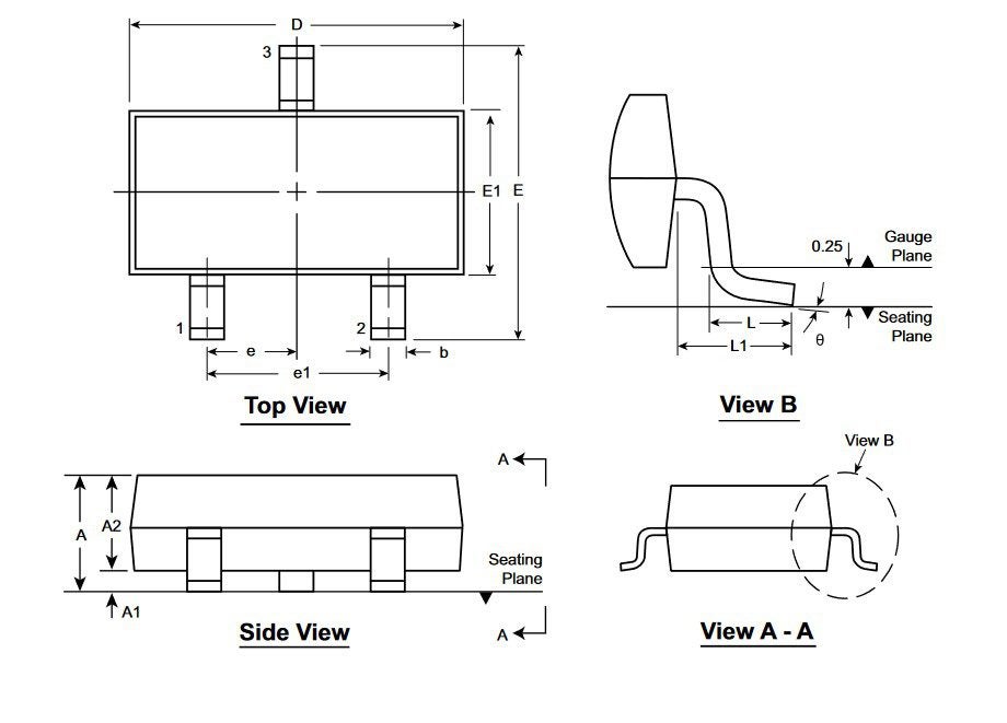
You can refer to the 2N7002 datasheet to view the min, max and nominal dimensions of the package for space optimization on your board.
To make the best use of the MOSFET, you will need CAD models and/or design data for other associated components in the circuit. Ultra Librarian can help you save time by enabling you to find all data in one place. Working with Ultra Librarian sets up your team for success to ensure streamlined and error-free design, production, and sourcing. Register today for free.


")