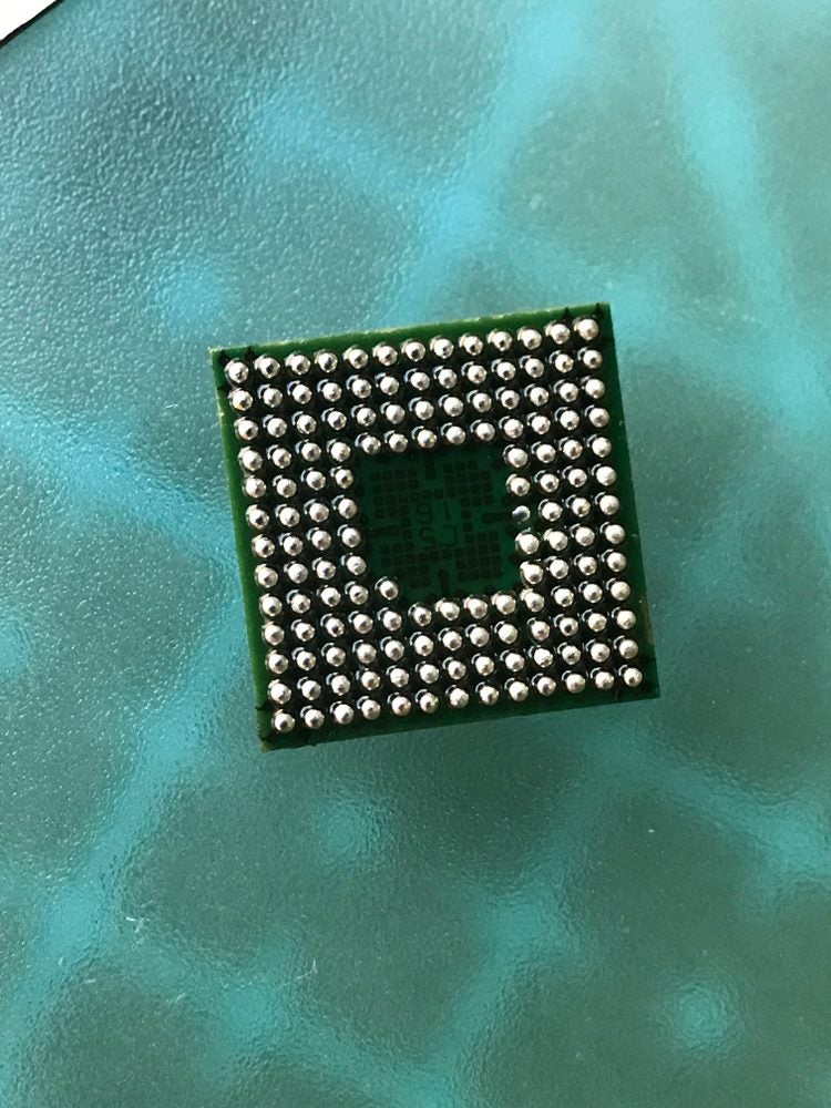
Flip chips are the most sophisticated BGA (Ball Grid Arrays) packages that eliminate the need for the typical bond wire required to connect the silicon diode with the lead frame. IBM introduced flip chips in 1962 to achieve more connections in ceramic substrates.
Initially, they were used for peripheral packages but quickly progressed into area arrays. Nowadays, most computing microprocessors we see- laptops, desktops, or servers – are flip chip bonded. Flip chip BGAs feature reduced board size, less height, lesser weight, greater I/O flexibility, and improved performance than typical BGA package designs.
Flip Chip Vs Typical BGA
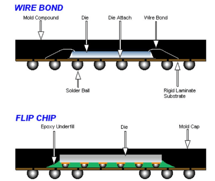
The die is attached to the substrate through a wire bond in a typical BGA package. Bond paths add inductance to the path and create EMI emissions. They also add resistance that significantly affects efficiency and power density, further worsening the EMI emissions. All these scenarios cease to exist in flip chips as the active area of the chip is flipped over and soldered directly to the lead frame, as in Flip Chip BGAs. It shortens the path by a form factor of 25 to 100. The best part is that the bonding can happen with the motherboard without requiring a substrate.
A flip chip package offers many I/O connections within a small chip area. The chip with metal bumps is flipped and processed through an oven- marking all connections simultaneously. However, in the case of wire bonding, connections are performed in sequence.
Flip Chip BGA Process
Step 1: Bumping the Die
The connection pad (chip front side) is coated with a metallic layer before adding soldered bumps. The process is called Under Bump Utilization (UBM). This layer hermetically seals the aluminum pad against oxidation and prevents metal diffusion from soldered bumps into the IC package. Now solder is deposited over the chip through various methods (electroplating, evaporation, needle depositing, etc.), followed by etching and reflowing the bump till it attains the shape of a ball.
Step 2: Attachment to the Die
The chip is flipped over, and metal bumps perfectly align over the substrate with corresponding pads (interconnection points).
The bumped die is then passed through a hot air reflow oven. The balls are slightly melted and reflowed until their bottom flattens a bit to form the connection with substrate. It ensures an electrical path with lesser impedance and lesser inductance. Solder flux is also applied to remove oxides and ensure perfect wetting.
Step 3: Epoxy underfill
An epoxy underfilled is required to compensate for any thermal expansion difference between the chip and substrate. Epoxy is needle-dispensed along the edges of each chip and is drawn into the under-chip space by capillary action. The setup is heat-curated to form a permanent bond. The underfill also protects bumps from moisture and other environmental hazards while providing additional mechanical strength to the assembly.
Flip Chip BGA Best Layout Practices
Land Patterns
Two types of PCB land patterns can be used during board design considerations:
- Non-solder Mask defined (NMSD): smaller metal pad opening as compared to the solder mask opening
- Solder Mask Defined (SMD): smaller solder mask opening than the metal pad
Any size mismatch can stress solder balls, leading to cracks. NMSD offers strong bonds and provides more room for escape route routing. However, too dense routing can also lead to short circuits during ball attach and reflow.
SMD offers better copper adhesion and compact placement of solder balls. However, larger copper pads can make the routing difficult.
Signal Line Space and Trace Width
Escape routing depends on trace width and min space required between two traces. By reducing the trace and space size, you can increase the number of traces. This can reduce the number of PCB layers and decrease the overall price. On the contrary, the board price may go up with shortened line width, and the performance quality will be compromised.
Vias
Vias are drilled holes that offer signal transfer between the layers of a multi-layer PCB. There are three types of vias as shown in the image below:
- Through via: Top to bottom
- Blind via: from top/bottom to an inner layer
- Embedded via: interconnection between any two inner layers
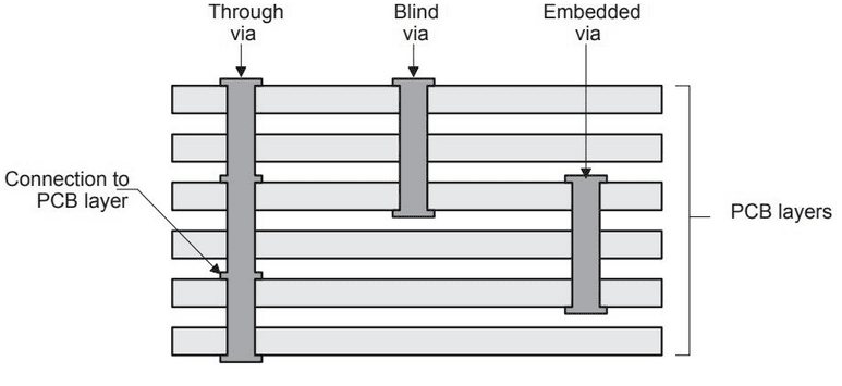
Blind vias reduce overall cost as the signals can be traced under a via, thereby minimizing the number of PCB layers. However, through-hole vias offer great design flexibility.
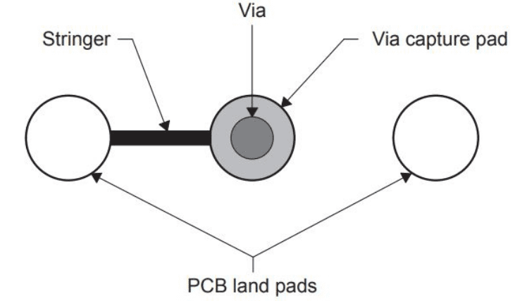
It is also a best practice to place vias inside a copper landing pad (via pads) to reduce routing space and overall manufacturing cost. Via capture pads and surface land pads are electrically connected through stringers.
 The table below shows the typical via capture pad sizes used by PCB vendors.
| Specifications | Typical (mils) |
| Trace/space width | 5/5 |
| Drilled hole diameter | 12 |
| Finished via diameter | 8 |
| Via capture pad | 25:5 |
| Aspect ratio | 7:1 |
Thermal Vias
Thermal vias offer an escape route for the heat generated to maintain a uniform temperature distribution across the PCB. For an optimal thermal performance, three essential thermal via design considerations are:
- Number
- Size
- Construction
These elements can impact PCB thermal resistance. To exactly determine the number of thermal vias required, you need to do characterization of the heat-removal efficiency versus the thermal via copper surface area.
Other Thermal Management Options
All connections take place at the bottom and the top side is available for heat dissipation. The top side is bare silicon with a superb thermal conductivity of 120 watts/meter-kelvin. Thus, most flip chips come without any mold compound over them for heat dissipation.
Nevertheless, you can opt for different thermal management options for flip chip BGA packages such as:
- Bare package with moderate airflow within a system
- Passive heat sinks + moderate airflow
- Active heat sinks
Adding thermal balls to a spreading plane in PCB in conjunction with thermal vias offers even better thermal performance.
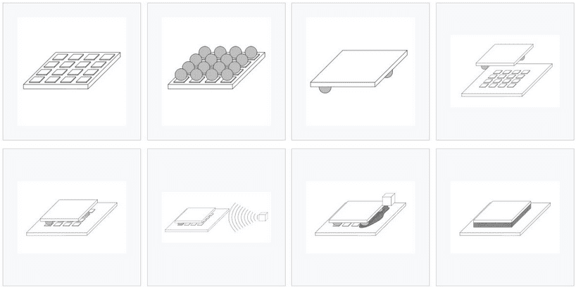
SMT Assembly – Tips & Best Practices
The typical SMT assembly process for flip chip BGA packages goes through several steps as shown below.
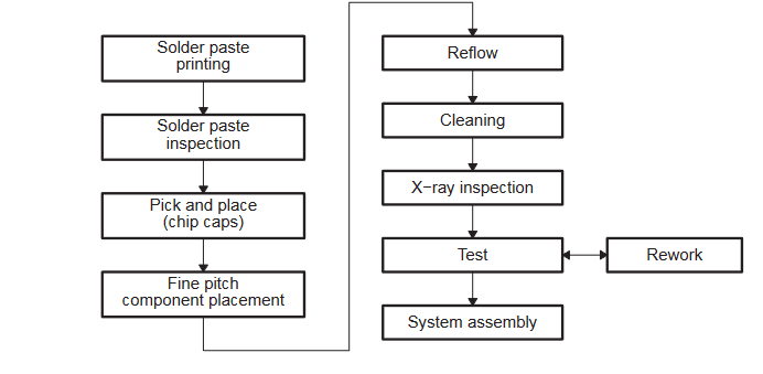
Using automated equipment for assembly and adhering to best SMT assembly considerations significantly lowers the production cost, optimizes cycle time and improves end-product quality. In this regard, here are some best industry practices:
- The front end of the board should have a straight and square edge to be easily detected by machine sensors. Irregular boards are expensive to assemble.
- To aid pick-and-place and printing machines, use minimum two or three fiducials (reference pads). They guarantee accuracy of placement.
- Maintain a minimum space between land areas of adjacent components to avoid shorting. Make sure no
- Add polarization symbols next to the positive pin of discrete components such as diodes and capacitors.
- The solder paste must have uniform viscosity and texture. Care must be taken to avoid drying out on the stencil.
- Forced convection is the most widely-accepted suitable reflow method for SMT packages.
- During solder reflow, temperature should be evenly applied from both sides of the PCB to avoid warpage (altered PCB shape).
- During solder reflow, allow sufficient warm-up time for the solvent to safely evaporate. Too slow or too fast curing can lead to solder-particle splatter or trapped gas, leading to voids and embrittlement.
- Maintain an even temperature across the board and package during reflow cycle to avoid uneven solder thickness and non-uniform solder joints.
- Check for verified CAD step files to keep the design compliant to the highest electronics standards.
Ultra Librarian seamlessly integrates with popular CAD/ECAD applications to help you better optimize your design process. Working with Ultra Librarian sets your team up for success to ensure any design is going through production and validation with accurate models and footprints to work from. Register today for free.