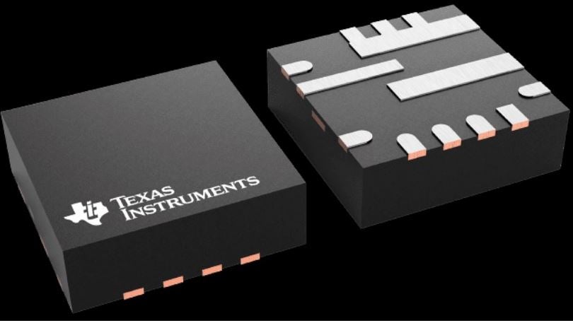
TI’s TPS56637RPAR Synchronous buck converter
If one aspect of circuit operation had to be selected as the most important, effective power management would be the choice. In addition to essential passive components, like resistors and capacitors, today’s circuit board’s invariably include active components and integrated circuits (ICs). Many discrete parts, like amplifiers, come in integrated circuit or IC packages with specific power requirements that must be supplied for operational integrity of the circuit and/or PCB.
For circuit boards, AC to DC or DC to DC converters are typically implemented to ensure the electrical supply for components and packages satisfies demand. A common type of converter is the synchronous buck converter. One of the most implemented of this type of converter is the TPS56637RPAR from Texas Instruments, Inc.
TPS56637RPAR: Features and Applications
The TPS56637RPAR synchronous buck converter has a wide input operating range from 4.5 V to 28 V. This converter is a high efficiency device comprised of integrated MOSFETs. Notable features and common applications are listed below.
As shown above, the TPS56637RPAR is a good general purpose converter that can be used in various applications.
TPS56637RPAR: Electrical and Thermal Information
Familiarity with device characteristics, as detailed in the TPS56637RPAR datasheet, is important for incorporating the converter into your design.
Constraints and Recommendations
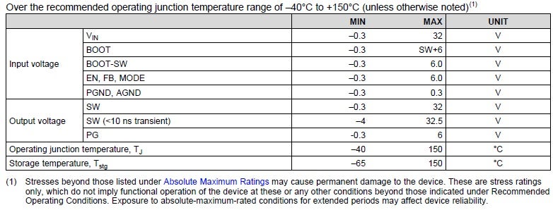
Maximum ratings for the TPS56637RPAR
In addition to the constraints above, the manufacturer recommends complying with the following operational requirements.
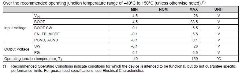
Recommended operating ranges for the TPS56637RPAR
Specifications
The following electrical and thermal parametric specifications should guide your PCB design with the TPS6637RPAR.
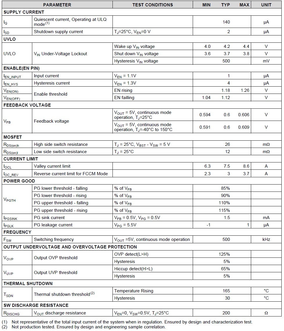
TPS56637RPAR electrical specifications
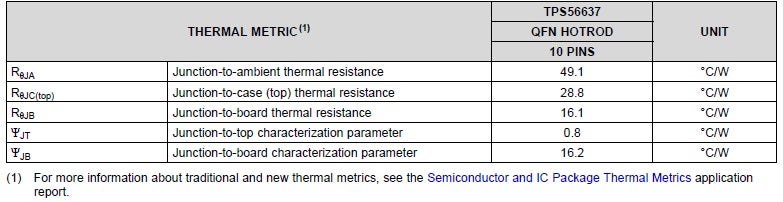
TPS56637RPAR thermal specifications
TPS56637RPAR: Architecture and Operation
The TPS56637RPAR datasheet also provides details about the converter’s layout and operation, which is essential for effective design and implementation.
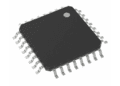
Pinout and Descriptions
As shown below, the TPS56637RPAR comes efficiently packaged in a HotRod QFN to optimize thermal management and minimize board real estate usage. These efficient operation attributes are augmented by monitoring and control capabilities for voltage, current and temperature to prevent device malfunction.
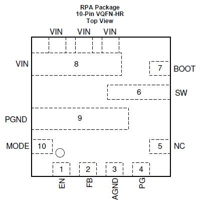
TPS56637RPAR pinout
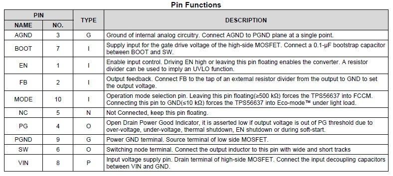
TPS56637RPAR pin descriptions
Diagram and Functionality
The function diagram for the device is shown below.
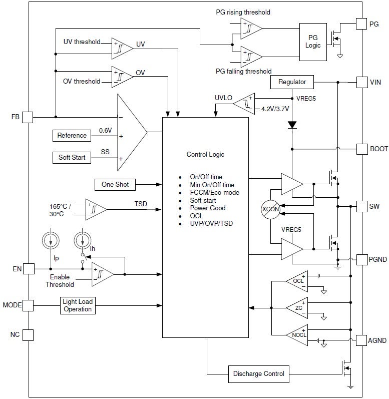
Functional block diagram of the TPS5667RPAR
The TPS5667RPAR is designed to provide reliable power control for connected loads with minimal external circuitry requirements. Additionally, seamless transition between high and low load operations.
TPS56637RPAR Operation Modes:
- Normal Operation
This is the typical operation mode for the converter. In this mode, the switching frequency is 500 kHz and continuous conduction occurs.
- Light Load Operation
For light load operational efficiency, forced continuous conduction mode (FCCM) is invoked by allowing pin 10 to float. Additionally, ECO-mode can be selected during which unnecessary internal functionality is turned off to aid in stability for light loads.
- Standby
When selected, all switching is suspended and the device current drops to the shutdown value of approximately 2 µA.
PCB Design With the TPS56637RPAR Datasheet
The TPS56637 datasheet is an invaluable resource for efficient and effective board design with this synchronous buck converter. In addition to design specifications, functionality, and operation, as discussed above, a suggested procedure for PCB layout design that should be integrated with general best practices, is included.
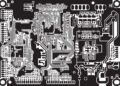
An example layout design (below) is also provided for guidance with your design.
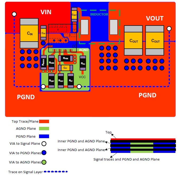
Example layout for the TPS56637RPAR
Your ability to leverage the wealth of device information and design data given for the TPS56637RPAR rests on your choice of an accurate CAD model, as shown below.
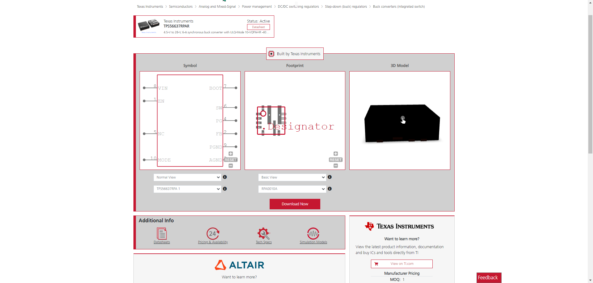
TPS56637RPAR CAD models from Ultra Librarian
If you’re looking for CAD models for common components or important design information on how to best use the TPS56637RPAR datasheet, Ultra Librarian helps by compiling all your sourcing and CAD information in one place.
Working with Ultra Librarian sets up your team for success to ensure streamlined and error-free design, production, and sourcing. Register today for free.