Accurate PCB antenna footprints enable designs that facilitate reliable wireless communication.
Depending upon where you live, the sight of rooftop and/or tower antennae is a familiar one. These structures are critical elements that enable wireless communication of various forms of data. Equally important are the much smaller antennas that directly interact with electronic circuit boards. At times, this is done through signal connectors; however, many electronic products employ on-board transmission/reception (TX/RX) devices. For these designs, it is imperative to understand the PCB antenna footprint types and best practices.
Why Are PCB Antenna Footprints Important?
It may be odd to think of antennas as PCB components, yet many of them are. Similar to other components, PCB antennas are defined on your board by their footprint, which significantly impacts their performance as shown below.
PCB ANTENNA FOOTPRINT ATTRIBUTES | ||
ATTRIBUTE | Description | Impacts |
Shape | Shape is the physical 2D geometry of the footprint |
|
Length | The distance between positive and negative connections. |
|
Spacing | The distance, both creepage and clearance, from other conductors | |
Orientation | The direction from which the antenna transmits or receives signals |
|
Pin/Pad Locations | Copper connection points |
|
Reference Designator | A soldermask label that identifies the placement location for a particular component |
|
As described above, PCB antenna footprint attributes significantly affect the design process and how well the component performs. To maximize antenna performance for your product/project, you must first choice the right antenna type.
PCB Antenna Footprint Types
PCB antennas come in an array of sizes and shapes depending on their operational objectives and where and how they are installed. Popular geometric shapes are the dipole, loop, and patch shown below.
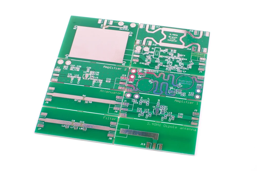
Various PCB antennas
The antennas above, as well as other common PCB antennas, are listed below, based on how or where they are typically applied.
PCB ANTENNA TYPES AND APPLICATIONS | ||||
Antenna Type | Common Applications | Antenna Type | Common Applications | |
Monopole |
|
Dipole |
|
|
Loop |
|
Patch |
|
|
Planar Inverted F Antenna (PIFA) |
|
Meandered Inverted F Antenna (MIFA) |
|
|
Flex Antenna |
|
Ceramic Chip Antenna |
|
Clearly, PCB antennas can be applied to products across several industries; including consumer electronics, communications, medical devices, automotives, and aerospace. Typically, these components are implemented where size is at a premium. Consequently, it is important to employ best practices for PCB footprint, as well as antenna-specific guidelines, as discussed below.
Optimizing PCB Antenna Footprint Effectiveness
When designing circuit boards with an antenna, it is imperative to follow design guidelines, such as isolating your antenna from other components and using solid ground planes. Additionally, optimizing the footprint of your antenna by incorporating the following footprint-specific considerations into your design process should also be a goal.
How to Create the Best PCB Antenna Footprint
📶Choosing the right antenna for your application The first step in choosing the best antenna for your design is to understand the various types available. Next, aligning the antenna attributes with your specific application and ensuring adequate space is available are critical to ensure your performance objectives are achievable. 📶Getting Accurate PCB Antenna Data and Information Accurate component data is essential for an effective PCB design workflow. This is especially true for antennas, as there are typically important manufacturing considerations, such as copper pours, keepouts, and other requirements that will degrade the performance of the device and your product, if not followed. 📶Laying Out Your PCB Antenna Circuit As radiators, antennas are subject to passing high currents, generating excessive heat, and creating substantial EM waves that may interfere with other on-board components. Consequently, it is important to follow good PCB layout guidelines, especially ensuring adequate spacing. 📶Ensuring EMC Compliance In addition to on-board EMI concerns like noise, boards with radiators are subject to compliance standards; such as IEC 6100 series which provides guidelines for EMC compliance. |
Awareness and adoption of the guidelines and suggestions above will not only contribute to an optimal PCB design workflow, but will also help ensure other development stages like fabrication and assembly proceed efficiently. The importance of accurate component data and information; such as manufacturer-vetted CAD models and available datasheet information, is key. The best option for meeting this criterion is to rely on the industry leader that more engineers choose for their component data resources, Ultra Librarian.
If you’re looking for CAD models for common components or important design information for maximizing the effectiveness of your PCB antenna footprints, Ultra Librarian helps by compiling all your sourcing and CAD information in one place.
Working with Ultra Librarian sets up your team for success to ensure streamlined and error-free design, production, and sourcing. Register today for free.