EMI Design Guidelines: Best Practices

EMI design guidelines should include good thermal management

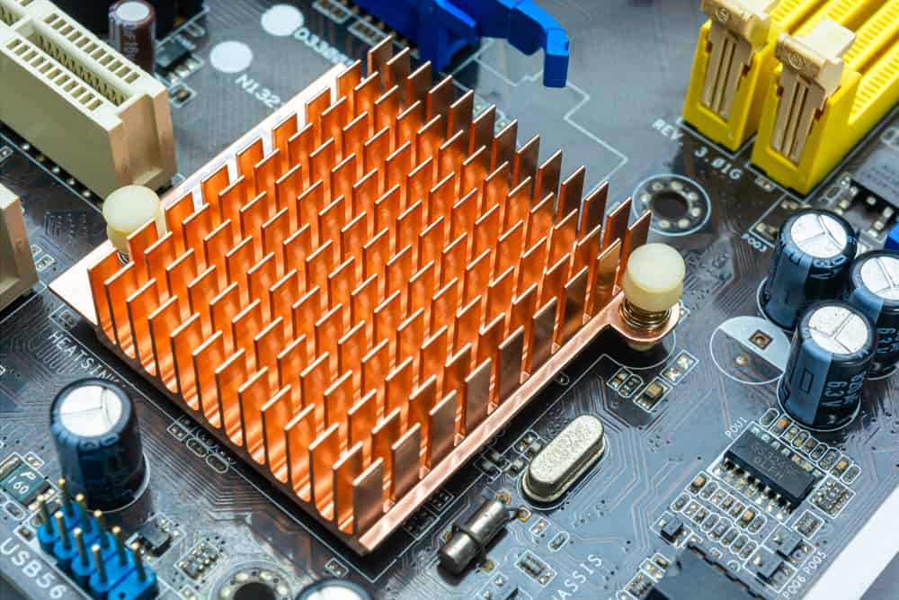
Good thermal management is a part of good EMI design guidelines

Ask any RF engineer or circuit board designer about their most challenging task, and you’re likely to receive a unanimous answer: minimizing noise or electromagnetic interference (EMI). Addressing this issue is undeniably the most difficult aspect of their work. Nevertheless, it is crucial to tackle EMI head-on due to its significant impact on the signal integrity (SI) of your board. Ensuring reliable operation and acceptable performance necessitates resolving EMI-related concerns.

While power integrity (PI) is often regarded as a separate matter from SI, it is important to recognize their intricate relationship. Overlooking proper thermal management methods can exacerbate your EMI problems. To achieve the best possible outcomes, it is imperative to adhere to EMI design guidelines that encompass all aspects of PCBA design affecting SI/PI.

PCB Design Considerations for EMI Minimization

Noise or electromagnetic interference (EMI) can be defined as unwanted electrical or magnetic energy in locations where it should not exist. In the context of electronic circuit boards, this refers to energy within the PCBA structure, on its surface, or nearby that can adversely affect the board’s signals. The latter scenario, often caused by nearby PCBAs or electronics, is typically categorized as an electromagnetic compatibility (EMC) issue. Mitigating PCB EMI and EMC concerns necessitates adherence to well-established design guidelines.

To achieve optimal EMI design, it is essential to consider the following factors and incorporate them into the design process.

Considerations For PCBA EMI Design Guidelines

Design Consideration

Why It’s Important

Component Placement

Components, especially high pin-count ICs, are a primary source of coupling and EMI on PCBs. Spacing between parts also defines trace separation at the source and termination points.

Trace Routing

Balanced mutual coupling between differential RF traces is good as it cancels interference. However, unbalanced differential routing and coupling of different signals will degrade SI/PI. 

PCB Stackup

A good stackup design helps with grounding and impedance control while minimizing PI degradation due to transients.

Impedance Control

Matching impedance is critical for RF routing, power transfer, and good SI. 

Filtering

Filtering is one of the most common methods of controlling EMI; however, choosing EMI components and placement locations is a design issue.

Grounding

The types and location of ground pads, planes, and traces, is foundational for circuit design. Bad designs can not increase EMI but also create issues like stray capacitance.

Shielding 

Instead of routing unwanted signals to the ground, shielding is an effective means of blocking radiated EMI and isolating the EMI source from other board elements.

Thermal Management

Heat is energy and can generate/increase unwanted current flow. Therefore, preventing hot spots and removing excess heat efficiently help minimize EMI.

EMI minimization is a multifaceted challenge, as evident in the table above, with numerous potential sources. It is important to acknowledge that completely eliminating unwanted signals and radiation from your board is highly unlikely, given that the fundamental operations of electronic circuits generate electrical and magnetic fields. However, the adverse effects on signal integrity (SI) and power integrity (PI) caused by EMI can be significantly mitigated by following effective EMI design guidelines.

EMI Design Guidelines for SI/PI Optimization

To optimize SI/PI and ensure the successful attainment of your PCBA’s operational goals, it is crucial to address and control various forms of EMI, including noise, ringing, ripple, inductive and capacitive coupling, and other sources. Although challenging, adhering to the following best practices for EMI minimization will help alleviate any substantial negative impact on your board’s functionality and structural integrity.

Best Practices for Minimizing EMI on Your Circuit Board

Component Placement

Trace Routing

  • Space traces for different signal types away from each other

  • Use differential pairs for high-speed signals

  • Use minimal spacing between traces within a differential pair

  • Make sure differential pairs have the same impedance

  • Avoid sharp (90°) corners within traces

Stackup

  • Do not put signal layers adjacent to each other

  • Route traces from differential vias on the same layer

Impedance Control

  • Make sure that differential traces have matched impedance

  • Ensure that outputs impedance and signal transfer channels (e.g. cables) have matched impedance

Filtering

Grounding

  • Use ground planes as opposed to ground pads, if possible

  • Use separate ground planes for different power sources

  • Keep ground returns as short as possible
  • Ground copper fill areas

Shielding

  • Use Faraday cages or metallic shields around high-voltage radiators

  • Use guard rings around components/circuits with large voltage potential differences

Thermal Management

Following the guidelines listed above will go a long way in ensuring that your PCBA does not suffer from excessive EMI.

If you’re looking for CAD models for common components or design information on the most effective EMI design guidelines, Ultra Librarian helps by compiling all your sourcing and CAD information in one place.

Working with Ultra Librarian sets up your team for success to ensure streamlined and error-free design, production, and sourcing. Register today for free.

UL-Icon.png

The Ultra Librarian Team

Ultra Librarian offers the world’s largest PCB CAD library, putting cutting-edge materials at your fingertips so you can build better products faster—all for free.

Join Our Newsletter

Subscribe to our newsletter to receive the latest news, and important updates

Name(Required)

Related Posts

If you’re looking for any of our component footprints or models, we have readily available and free options for you and your design team. Search our library for the solution you’ve been looking for.

Free Design Resources

Ultra Librarian is the worlds largest online – and always free – PCB CAD library. Build products better, faster, and more accurately with easy access to vendor-verified symbols, footprints, and 3D models. Register today to start searching the right components for your next design.

Recommended