Thermal management of electronic device analysis
The increased utilization of electronic circuit boards, which continues to grow every day, can accurately be called a technological revolution. This revolution, driven by demands for greater functionality and capabilities, has produced intelligent devices, autonomous systems, and interconnected networks that span the globe and connect us to space. And designing and building the electronics for these advancements necessitates that engineers, designers, ODMs, and OEMs emphasize the critical power components that drive them.
ICs are getting smaller while power requirements are going up simultaneously to accommodate the various power needs of more complex circuit architectures. More components mean more power, which translates into more heat. Managing the heat generated by high power components is critical, which necessitates successfully addressing power density issues. Solving the problem of effective thermal management of electronic devices has long been on the radar for Texas Instruments, resulting in advanced packaging technology that enables the continued development of innovative high power electronics.
Understanding the Thermal Challenges for High Power Electronics
The greatest constraint to technological innovation for high power electronics lies in the physical limitations of the materials and devices. This boundary, although unbreachable without the introduction of new materials, can be reached by design and manufacturing optimization. Doing so requires understanding the issues that most affect power management, as listed below.
| POWER MANAGEMENT CONCERNS | |
| Issue | Need |
| Protection and accuracy | Accurate power integrity (PI) and signal integrity (SI) and low noise operation. |
| Isolation | Reliably transferring power across high voltage barriers. |
| EMI | Minimizing EMI with tighter specs and in smaller areas to satisfy standards and reduce costs. |
| Battery life | Self-power applications require achieving a low current quiescent point, especially during no-load conditions. |
| Power density | Enabling high power operation in smaller areas to increase functionality, efficiency, and lower costs. |
All of the above are important, and your design likely necessitates that you prioritize one or all of these concerns. However, the trend towards more compact boards makes addressing power density critical for the thermal management of electronic devices.
Methods for Electronic Device Thermal Control
Heat is an inevitable byproduct of electronics. Therefore, employing some form of thermal management is necessary for virtually all ECAD/MCAD system designs. As excessive heat comes from power losses in the system, techniques for addressing thermal management are typically based on the following strategies.
Thermal Management of Electronic Devices Techniques
- Expand Heat Distribution Area
Heat transfer is limited by area. Consequently, increasing board size results in wider heat distribution, lessening heat intensity, and lowering the probability of adverse effects, such as erroneous circuit behavior and damage to components.
- Increase Heat Dissipation Abilities
When board space is not an option, dissipating heat from compact areas quickly is critical. Popular techniques to achieve this are using heat sinks on the top or bottom of components and using vias-provided ample layers available in the PCB stackup.
Often power density constraints, such as component package size and enclosure parameters, force designers to choose a less-than-optimal technique for thermal management, resulting in limitations on design flexibility and PCB utilization. TI has developed advanced solutions incorporating both techniques for optimal thermal management of electronic device solutions for increased power density applications.
Advanced Thermal Management of Electronic Devices
Improving power density is the key to facilitating greater electronic system functionality and capability and increased application of smaller form factors. For high power applications, this is predicated on optimizing power conversion efficiency. To a great extent, choice of components influences power conversion performance for your design. And component packaging is one of the principal areas of focus for TI’s thermal management of electronic devices solutions, which has resulted in several innovations, as shown below.
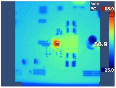
Thermal profile for TI’s HotRod QFN packaging.
As shown in the figure above, TI’s HotRod™ packaging –which eliminates the need for wire-bonding in QFNs–maintains the temperature for the device and surrounding board area within safe limits. This packaging takes advantage of the thermal advantages of flip-chip technology. However, this packaging technology has been improved to allow for larger die attach pads (DAPs). The result is much better thermal performance, as illustrated below.
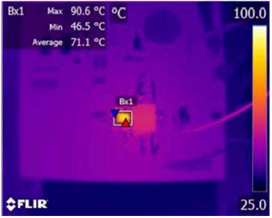
TI’s enhanced HotRod QFN thermal profile
As shown for the LM60440 synchronous converter, the average temperature has been reduced to lower than mid-range for safe operation. These advancements offer the following advantages for improving thermal performance in high power applications.
Benefits of TI’s Advanced Packaging Technology for Thermal Management of Electronic Devices
- Better thermal dissipation
- Lower losses through switching
- Better top-side heat sink attachment
- Smaller footprints
These significant advantages can be maximized by coupling the implementation of this packaging technology with good thermal design practices, simulation, and testing.
If you’re looking for CAD models for common components or advanced solutions to challenges like thermal management of electronic devices, Ultra Librarian helps by compiling all your sourcing and CAD information in one place. Working with Ultra Librarian sets up your team for success to ensure streamlined and error-free design, production, and sourcing. Register today for free.