
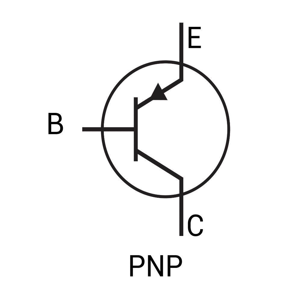
An NPN transistor is suitable for low voltage switching applications. However, using it for HV applications requires additional setups, such as drivers, to maintain the minimum base-emitter potential (0.7V) for switching. In addition, the methods used are complicated and costly. Instead, a PNP transistor is used for circuit simplicity.
Unlike in an NPN transistor, it is easier to keep the base at a low potential than the emitter in PNP configuration to turn the device ON. In this regard, the 2N5401 is a high voltage and low current switching transistor also used for telephony applications. Therefore, understanding the 2N5401 datasheet and its applications can help you quickly meet some specific HV applications.
How to Use 2N5401 Transistor HV Applications?
The 2N5401 PNP transistor is helpful for high voltage – low power switching and amplification applications. The best example is telephone systems where the current demand is low (max. 300 mA), and the operating voltage is 150 V or below. As the collector current is 600mA, it can easily control relays, LEDs, and other transistors in the circuit. Alternatively, it can also be used in power audio amplifiers.
The complementary NPN pair for a 2N5401 PNP transistor is 2N5551. A complementary pair of “NPN” and “PNP” transistors helps design power amplifiers. Power amplifiers, such as Class B amplifiers, help drive current through the load (e.g., motors) in both directions to facilitate forward or reverse operations. In addition, the transistor is cheap and readily available.
Analyzing 2N5401 Datasheet
2N5401 Pinouts
When you face the flat edge of the transistor, the rightmost lead represents the collector, the middle one is the base, and the left-most lead is the emitter, as shown below.
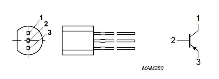
| Pin | Name | Function |
| 1 | Emitter | Current incoming pin |
| 2 | Base | Triggers transistor ON/OFF |
| 3 | Collector | Current outgoing pin |
Technical Specifications
| Name | Description |
| Max VCE | 150 V |
| Max IC | 600 mA |
| Max VCB | 160 V |
| Max VBE | 5 V |
| Operating Temp Range | -55ºC to +150ºC |
| Max Power dissipation PC | 0.62W |
How does 2N5401 Transistor Work?
Let’s not forget that it’s a PNP transistor. As the base has N doping and the emitter has P doping, the base is maintained at a negative potential concerning the emitter to turn the transistor ON. Also, the emitter supply voltage is kept positive concerning both collector and base. Finally, a limiting resistor connected at the base helps limit the base current to its maximum value.
If you look at its general switching application shown below, it receives current through the emitter. Thus, it is connected to the positive terminal of the battery. The base is connected to the negative terminal of the battery. In this configuration, the transistor gets activated (turns ON).
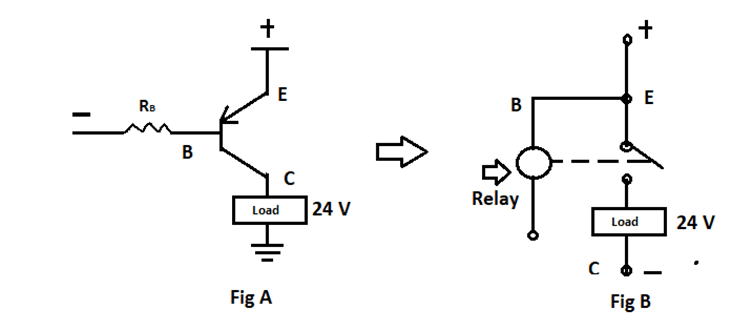
The diagram in Fig A shows how a 2N5401 PNP transistor is driving a standard load of 24 volts. Diagram B gives a more vivid image of the switching phenomena.
A relay at the base can act as a switch to operate the load. When the base is at sufficient negative potential such that VBE is greater than 5 volts, the relay operates and closes the switch. The current flows from the emitter and out of the base into the collector- as if both collector and emitter are shunted together. The collector current gets amplified and flows through the load. The amplification can be min 50 times to a max 240 times of the input current.
However, it is imperative to note that when the transistor is inactive, it does not turn it to 0 volts; it floats. To bring it to 0 volts, you must use an NPN transistor (sink) in pairs. The main difference between a PNP and an NPN transistor is that voltage polarities and current directions are opposite.
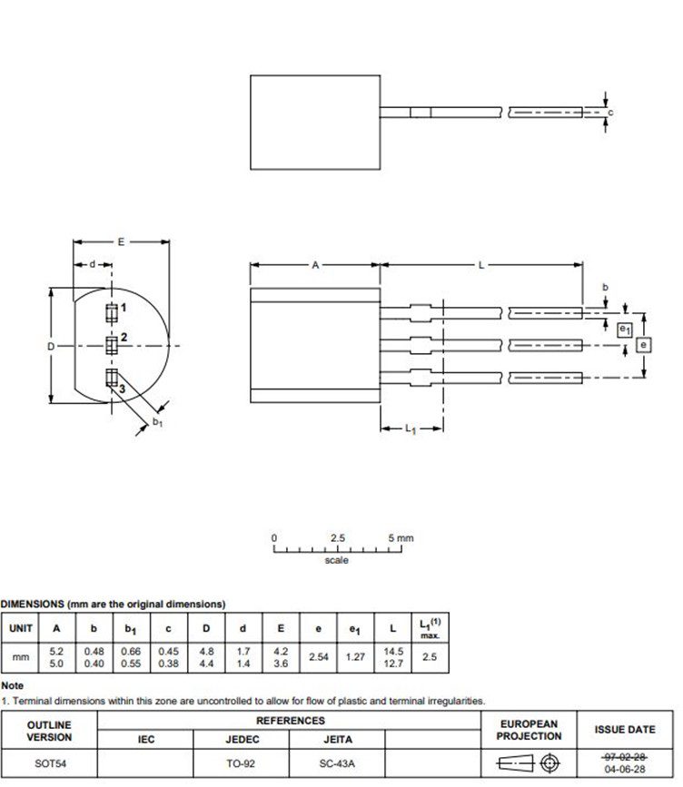
2N5401 Package Layout
The 2N5401 comes in a SOT54 (TO-92) plastic package. The compact size takes less space on the board. However, the lack of heat sink in the design makes them ineligible for high current applications. The package layout and dimensions are shown below in the 2n5401 datasheet.
2N5401 Alternatives
As we are talking about high voltage, low current PNP transistors, here are some ideal alternatives to 2N5401 transistors. They all have almost the same technical specifications as for the 2N5401 transistor, with some exceptions.
- MPSA93
- BF723
- 2N5096
- MPSA92
Using 2N5401 for any low current HV application requires a thorough understanding of the 2N5401 datasheet, footprints, application notes, and ECAD/MCAD models. Ultra Librarian can help you access all these pieces of information in one place. You can also quickly get the real-time availability status of your favorite component from different vendors to avoid supply chain bottlenecks.
Working with Ultra Librarian sets up your team for success to ensure streamlined and error-free design, production, and sourcing. Register today for free.


")


")