
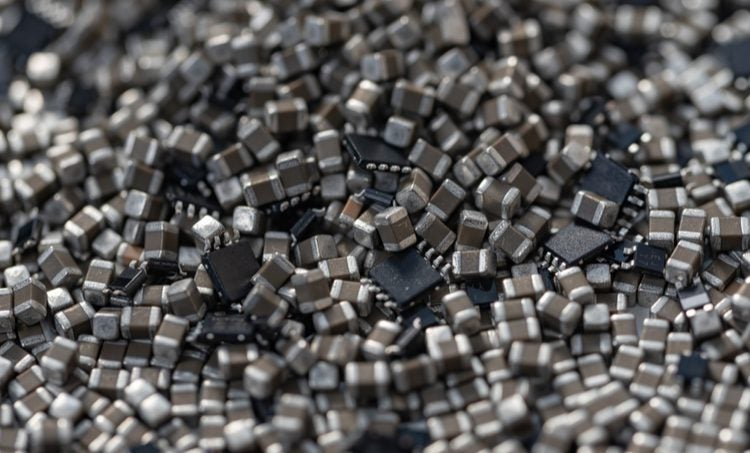
SMD components are not going away anytime soon, thanks to their low cost and low profile. SMD components come in a variety of standardized packages that make manufacturing and assembly with automated equipment much easier. The size of an SMD component can range from a large FPGA measuring inches across to a small resistor measuring just a couple mm. These components have standardized rectangular packaging, but they require small land patterns for soldering electrical connections on a PCB.
Where can you get the most accurate information on the land patterns you need to create for your components? If you download a component model from a forum or parts aggregator, the footprint may match the dimensions shown in SMD component datasheets, but the land patterns may need to be modified to prevent some common PCB assembly defects due to mis-sized lands. If you can access SMD component datasheets and verified footprints before you create your land pattern, you can prevent some extra engineering expense and ensure you comply with DFM guidelines.
Building Footprints vs. Land Patterns
The terms “land pattern” and “PCB footprint” for SMD components are sometimes used interchangeably, but they are not exactly the same. If you’re creating a model for 2D or 3D CAD models for a component, you need to differentiate between the body of the component itself and its land patterns. Note “land pattern” also applies to through-hole components, but it refers to the arrangement of holes for mounting the component on the board.
Here’s the difference between the two: the land pattern refers to the arrangement of pads (and possibly vias for fine-pitch BGAs) that are placed on the PCB. The footprint sometimes simply refers to the physical outline of the component, although it could also collectively refer to the combined land pattern + silkscreen outline/RefDes + courtyard + solder mask opening, all rolled into a single model. In some PCB design software packages, this is the meaning given to “PCB footprint;” you’re placing the land pattern, silkscreen information, mechanical outline, and courtyard definition in multiple electrical and mechanical layers in your design.
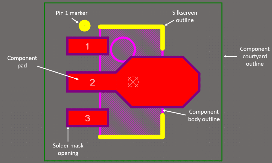
The image above shows all the different pieces of information that go into an SMD component. Obviously, an SMD component is more than its silkscreen outline and land pattern. What you also see is the landing pad size and solder mask opening, not the size of the leads. If you know what to look for in SMD component datasheets, you can easily build the right land patterns for your components.
What to Look for in SMD Component Datasheets
If you’re in the mood to create SMD component symbols and footprints from datasheets, you’ll need to remember the land pattern does not perfectly match the pad arrangement or body outline. The body dimensions of the component should be clearly listed in a mechanical drawing and can be easily replicated in your CAD tools. This will help you define the ideal silkscreen outline in your PCB footprint.
When drawing a landing pattern from SMD component datasheets, it’s important to remember the landing pattern in a datasheet is only a recommendation. Some datasheets will just show the pad sizes and will allow you to determine the best landing pattern. You’ll need to determine the best pad size in your land pattern and solder mask opening. Be sure your final footprint complies with the requirements for the standard you are working with: IPC-7351B as an industry standard, or perhaps internal/customer standards for a more custom package.
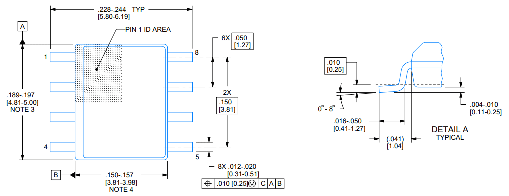
CAD drawing showing pad arrangement on the LM393BIDR from Texas Instruments.
The CAD drawing shown above is common in SMD component datasheets. The pad arrangement is not a land pattern, it’s simply a mechanical drawing that you can use to design a pad arrangement for your PCB footprint. The pads used for soldering and mounting on a PCB will extend outward around the lead outline. The distance between neighboring pads and the solder mask opening around each pads should be large enough to prevent bridging during soldering.
All information on lead sizes, package dimensions, and recommended landing pads can be found in SMD component datasheets. If you want to get accurate component models alongside datasheets and sourcing information, there are some online options for finding the data you need.
Get Your Datasheets and Component Models in One Place
If you’re looking for SMD component datasheets with accurate information and full electrical specifications, there are a number of resources available. Distributors will generally provide datasheets for most of the components they sell and larger manufacturers will make these datasheets available on their websites. If you need to compare component specs and prices, get aggregated sourcing data, and find component models, you need to use the right components search engine. These services aggregate these data in one place, giving you a one-stop shop for multiple parts.
When you use the parts search features in Ultra Librarian, you’ll have immediate access to verified PCB footprints, schematic symbols, and 3D models for your components. You’ll also have access to SMD component datasheets, and all at no cost to you. You’ll have everything you need to customize component models for your new board and import them into popular ECAD applications. You’ll also have access to sourcing information from worldwide distributors.
Manually creating design libraries for SMD components takes most teams dedicated resources and time, but Ultra Librarian helps by streamlining this process. Working with Ultra Librarian sets up your team for success to ensure any design is going through production and validation with accurate models and footprints to work from. Register today for free!


")
")
