When designing circuit boards, you are often faced with what seems to be a choice between “less is more” and “more is better.” The former is based on the fact that simple circuits or fewer traces are easier to design and build. The latter is rooted in the truism that multiple paths reduce the load on each.
The simplest example of multiple signal paths is differential pairs, which can be the better choice for your design—particularly for high-speed boards. Opting for this scheme begins with understanding the challenges of laying out signal paths. Then, follow differential pair routing guidelines that will optimize your board’s signal integrity.
Challenges of PCBA Signal Routing
PCBA signal routing is one of the major challenges of circuit board layout and design. In fact, trace concerns are central to all phases of board design. For example, during schematic capture, successful creation of the netlist—which is a listing of all wiring connections—is critical to proceeding to the layout design. The netlist serves as the blueprint for trace routing. Errors uncorrected may not be discovered until the board is built and tested.
Autorouting is a great tool, but it relies upon the accuracy and completeness of the netlist. In most cases, even with the best PCBA design software, some manual trace routing will be required. Therefore, the challenge is to ensure that all connections are made and the following objectives are met.
PCBA Trace Objectives
- 🡺 Adequately carry board currents
The first responsibility for all copper traces is to safely carry whatever currents are presented. This includes surface traces, vias, signal layers, and ground planes.
- 🡺 Support power integrity
Board currents can be classified as either signals or powers—including their returns. For power paths, it is imperative that components, devices, and loads are supplied with reliable electrical energy at the voltage and current levels required.
- 🡺 Maximize signal integrity
It is important that electrical parameters fall within ranges such that they are interpreted correctly. For example, digital signal amplitudes must be clearly distinguishable as highs and lows to identify bits. With RF signal propagation, transition speeds are equally important to reduce or eliminate reflections and other signal attenuation activity.
Successfully meeting these objectives necessitates your design to mitigate the greatest challenge to board design, especially for high-speed applications, which is EMI or noise. One method of addressing this problem is to employ differential pair routing.
Why Use Differential Pair Routing?
All RF signals require two lines—one for the signal and one for the return. For multilayer boards, the signal and return typically utilize two different layers (e.g. surface and ground plane). For differential pair routing, both paths are run adjacent to each other on the same layer. This reduces the amount of current on the ground plane, which is one of the advantages of using differential pairs.
| Advantages of Differential Pair Routing
👍 Minimum ground plane usage 👍 Common mode noise immunity 👍 Provides good reference for signal switching 👍 Increases signal-to-noise ratio (SNR) |
All of the advantages above work to address the EMI that can be created on your board. However, there are disadvantages to consider, as well.
| Disadvantages of Differential Pair Routing
👎 Impedance matching is necessary 👎 May require meandering or longer traces 👎 Uses more space on surface or signal plane 👎 Errors or mismatches can cause significant EMI |
If signal integrity is of primary importance and/or surface area is not as critical, you will likely benefit from differential pair routing. However, it is critical that you follow good guidelines.
Differential Pair Routing Guidelines to Follow
Effectively implementing differential pair routing means adopting the perspective that two is better than one for PCBA signal integrity, which is often true for high-speed boards. At high speeds, precise switching and constant impedance are mandatory and can be readily achieved by following the guidelines below.
Best Differential Pair Routing Guidelines
- Maintain equal spacing between traces
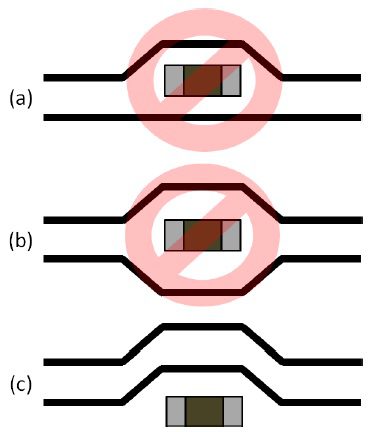
Maintaining differential trace symmetry. Image from TI.
- As shown above, only the example in (c) keeps the separation between traces constant
- even when running traces around components—or other board elements.
- Ensure trace lengths are identical
This requirement is also imperative. In certain cases, it may be necessary to employ meandering or serpentine routing to extend the length of one of the traces to match the other.
- Keep trace impedances constant
In addition to the two guidelines above, the traces must also have the same physical attributes. This includes size, width, copper weight, and thickness.
These guidelines are simple, but critical. Variation in either of these can significantly affect your high-speed signals and board performance. Another good rule of thumb when working with differential signals is to utilize matched components, preferably from the same manufacturer. These parts will be built to optimize processing of transmitted and/or received signals which will aid your board’s signal integrity.
If you’re looking for CAD models for common components; including matching TX/RX parts, or proven design tips such as differential pair routing guidelines, Ultra Librarian helps by compiling all your sourcing and CAD information in one place.
Working with Ultra Librarian sets up your team for success to ensure streamlined and error-free design, production, and sourcing. Register today for free.