
High speed telecommunications applications
It is always amusing when someone describes a previous state of technology as if it no longer has relevance. For example, the highly organized system of physically transporting information between two parties is often referred to as snail mail. Of course, snails traveling at the speed of planes, trains, and automobiles is an inconceivable natural phenomenon. Yet, the term has veracity when comparing the postal service to telecommunications for speed.
Telecommunications systems are the preferred method of conveying information – that can be converted into or represented by electromagnetic signals ranging from low frequencies to extremely high ones, as shown below.
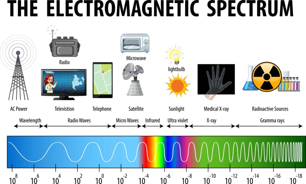
Telecommunication frequency ranges
The frequency at which signals are transmitted, received, and processed dictates how PCBAs are designed and built to operate the electronics that comprise telecommunications systems effectively. This is especially important for high-frequency signals that require high speed layout guidelines for telecommunications implementation.
High Frequency vs. High Speed Board Design
Although it is common to see frequency and speed utilized as if they are synonymous in electrical and electronics literature, this is not entirely accurate. Frequency, the inverse of the wavelength, refers to a signal’s location on the electromagnetic spectrum. Graphically, this is often presented by a periodic waveform (e.g., sinusoidal wave) as the time for a signal to complete a positive and negative transition and arrive at the same amplitude.
For radio waves, frequencies between 3 and 300MHz are considered high frequency and require those special design considerations, beyond best practices for PCBA layout and signal integrity, to be implemented.
High speed may indeed refer to signals in the high frequency range. However, speed is a classification based on signal transition or rise time (Tr) and propagation time (Tp) required for the signal to traverse the transmission path length–this is often referred to as propagation delay; however, the time for the signal to travel through a component; such as a shift register or NAND gate is also called propagation delay. If the ratio shown below holds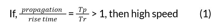 Then high speed layout guidelines for telecommunications are warranted for your board.
Best High Speed Layout Guidelines for Telecommunications
Before learning how to layout your high speed board, it is informative to understand why it is crucial and the challenges these boards present. Telecommunications systems generally operate with low-level signals. Amplitudes in the micro and millivolt range are standard.
Moreover, many system paths are wireless and travel great distances, where path loss and signal dissipation have a tremendous impact. It is also important to note that board build must be considered as well as signal integrity.
Challenges for High Speed Layout Design
- Signal degradation
The combination of low signal amplitudes and path losses may result in signals that are not read accurately. For example, signals that appear to be above an established threshold can be interpreted as highs; instead of lows.
- EMI and EMC
Noise from other signals on the board or from nearby circuit boards or other sources can distort signal fidelity and lead to erroneous operation.
- Signal reflections
Reflections occur when that is an impedance mismatch. For example, traces of different lengths or inconsistent separation between adjacent traces.
These challenges can be mitigated by following good high speed layout guidelines for telecommunications, as listed below.
How to Optimize Your High Speed Board Layout
- ➔ Use materials with a consistent dielectric.
- ➔ As much as possible, use straight line traces.
- ➔ Make sure that differential traces are identical in length and have consistent spacing throughout.
- ➔ Opt for low-profile copper.
- ➔ Apply termination techniques where warranted to ensure constant impedance.
By applying the suggestions listed, choosing your components well – for example, using matched TX/RX parts from a single manufacturer will aid you in meeting impedance matching requirements – and providing your CM with accurate CAD footprints and other data you can produce high-quality high speed boards for telecommunications applications.
If you’re looking for CAD models for common components and useful design tips, such as high speed layout guidelines for telecommunications PCBAs, Ultra Librarian helps by compiling all your sourcing and CAD information in one place. Working with Ultra Librarian sets up your team for success to ensure streamlined and error-free design, production, and sourcing. Register today for free.


")