Cell phone chargers are one of the most common uses of electronic rectifiers.
Some may say that love, money, or even coffee make the world go around. Engineers usually lean toward a more scientific answer, such as ‘power makes the world go around.’ There is a strong case for this perspective. Can you imagine what would result if we suddenly were without chargers to power up our cell phones?
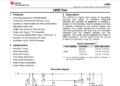
Fortunately, we have rectifiers that convert AC to the required DC level to power our products and systems. A typical example of this is converting the 120V/208V or 230V/400V AC from the power mains to the 5V DC necessary for cell phones. Here are several of the topologies available for electrical rectification:
| Common Rectifier Topologies | ||||||
|
All devices above are in power supplies or output control circuits. The design challenge is to select the best rectifier topology for your application, considering the required performance needs and characteristics.
The bridge rectifier is a good general choice for many applications due to its relatively constant (low ripple) output, efficiency, uncomplicated design, and low cost. However, to fully leverage these advantages, good PCB layout bridge rectifier design guidelines are necessary.
Important Design Guidelines for Bridge Rectifiers
Bridge rectifiers owe their moniker to their circuit architecture, an example of which is shown below for the MSB30M bridge rectifier.
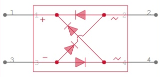
Schematic symbol for the MSB30M-13 bridge rectifier.
As illustrated, one two-diode pair (1 and 3) forms a bridge between the input and the output during one half-cycle, while the other pair (2 and 4) forms the bridge for the other half-cycle. Due to its relatively constant DC output, this rectifier configuration is a favorite for linear power supply designs. When designing bridge rectifier circuits, following the layout guidelines listed below is essential: