

Hobbyists and makers often have it easy when it comes to PCB designs. Even though they might build some fantastically engineered circuit boards and may function perfectly, these designs do not need to pass through rigorous EMC testing to be built or released to the market. Professional designers need to do more than check that designs work as intended; they need to ensure they emit low noise levels and unintentionally interfere with other devices. EMC design guidelines should be followed first to help ensure a product will pass EMC testing.
Although EMC testing is a bit complex, a board designer doesn’t need to know everything about EMC tests or how to analyze failures. However, they should know something about the basic board design guidelines that will help prevent excessive EMI, both on the board and noise emitted from the board. This article will cover some of the essential points that will help PCB designers ensure their products have a chance of passing EMC testing and complying with emissions regulations.
Getting Started With EMC Design Guidelines
EMC testing focuses on excess noise emitted from electronic systems as radiated and conducted emissions. These emissions are measured across a broad frequency range during operation, and regulatory bodies (e.g., FCC in the US or CISPR in Europe) define limits on noise that will leave a system through these two mechanisms. Designers do not necessarily need to know specific limits during a design, but they should be able to see what potential design choices will impact noise emissions.
The causes of EMI generated in a PCB layout will fall into four broad categories:
- Stackup design
- Routing and parts placement
- Switching signals (power and high speed)
- Shielding
Stackup Design
This is probably the most important set of design guidelines that can be implemented in a PCB. Most EMI problems originate directly from a poorly designed stackup, or the stackup will make an existing problem worse. Newer designers will almost always use 2 layers out of a perception of low cost without understanding the performance benefits, or they might use a 4-layer PCB stackup incorrectly. All of this is a recipe for an EMI failure.
The key to successful stackup design is placing planes and defining ground. Make sure to use ground planes to support routing, even though it will take up an entire layer. Using a single ground reference conductor throughout the system will help eliminate noise from ground potential offsets, and it will aid routing throughout the system. Ground also provides shielding against external EMI and ESD.
Routing and Parts Placement
If you’ve designed the stackup correctly, then you can more easily route everything correctly. Component placement will also determine where you need to route to ensure you can make the required electrical connections.
EMI from routing problems will arise in two situations:
- Routing across more than 1 layer through a via with no nearby ground
- Routing across a region of the board with no ground on the next layer
Routing over a ground plane is standard practice and should always be done unless you can prove otherwise. When routing between two layers through a via, make sure there is a ground via nearby to provide a clear return path and maintain low loop inductance. Both strategies will help eliminate most EMI problems that occur when routing, even at low signal speeds and low frequencies.
Switching Signals
Any signal that switches at fast edge rate has a chance of emitting radiation or conducting broadband noise at its fundamental frequency and its harmonics. Switching signals in PCBs come in two forms: digital bitstreams and PWM signals that modulate switching elements in power systems.
For digital signals, make sure you put these signals over a ground plane and route them properly as described above. In power circuits, it’s more complicated as you aren’t using traces to route output power. Instead, you will use planes or polygons, and the location of these nodes in the board should be kept separate from other circuits in the design. Spacing or additional ground pour between power circuits and other circuits will help reduce noise coupling from switching power regulator nodes into other circuits or components. This will then reduce conducted noise from the system and reduce radiated noise.
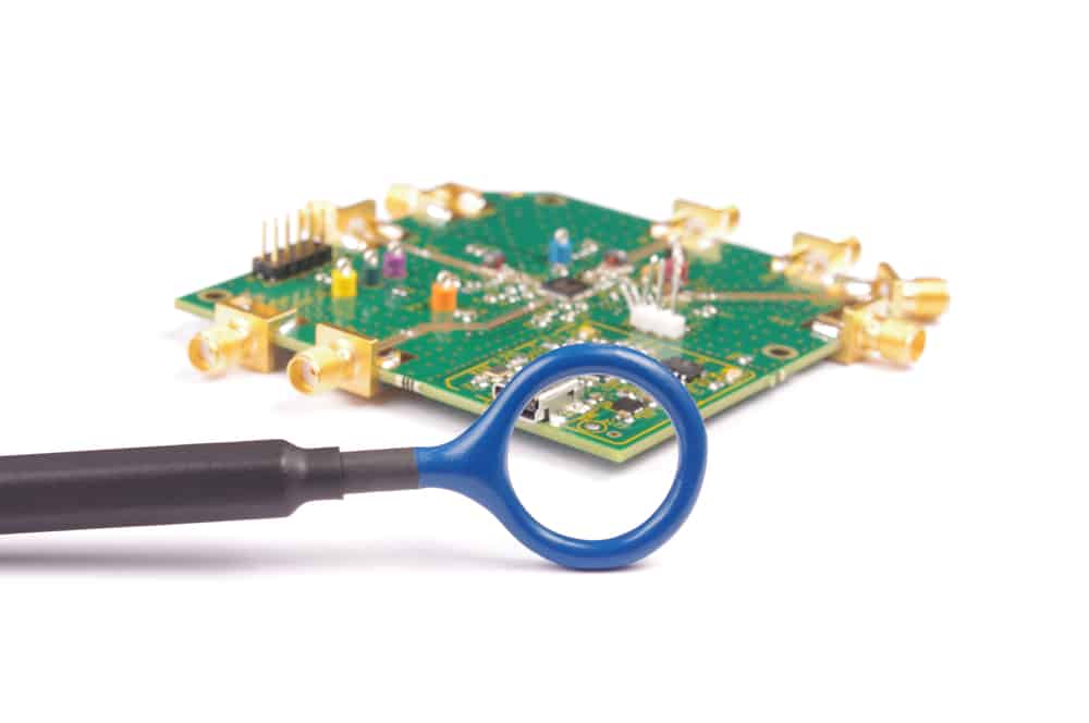
Use a near field probe with an oscilloscope to identify noise sources in your PCB.
Shielding
Most designers that have never had to solve a noise problem from a bad layout will probably look at shielding as the first resort to solving the problem. The reality is that shielding in the form of excessive copper, metal shielding cages, ferrites, shielded enclosures, shielding compounds, or any other method should be considered a last resort. Shielding doesn’t give you an excuse to create a bad stackup, layout, and routing strategy. If you are successful in all the areas outlined above, you probably won’t need additional shielding in most designs.
Although shielding shouldn’t be the first step to solving EMI problems, there are instances where you will need it regardless. For example, high power switching converters, certain RF systems, and mixed-signal systems that implement all the abovementioned points might still have radiated noise problems so they may need additional shielding. The nice thing about shielding components (metal cans, ferrite plates, etc.) is that you can experiment with them if a prototype fails EMC testing, and no other solutions can be determined so that you can experiment with different shielding measures as part of board debugging.
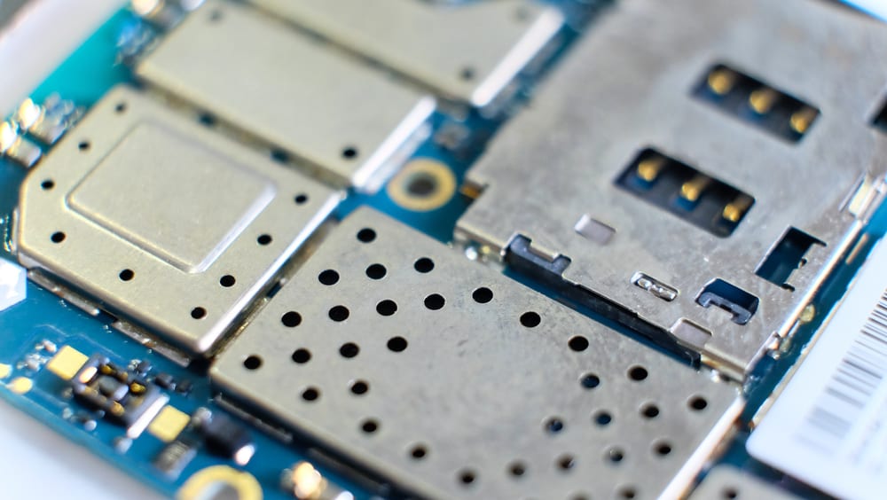
Shielding cans on a PCB are used in some mobile products that pack a lot of digital components and RF circuits into small boards.
Summary
The following table summarizes the basic steps you can take to reduce emissions from your PCB layout.
| EMI problems targeted | |
| PCB stackup |
|
| Routing/placement |
|
| Switching signals |
|
| Shielding materials |
|
Make sure to follow these EMC design guidelines to help make sure your next PCB passes compliance testing successfully. There are other part-specific guidelines to follow that we can’t address here due to space constraints, but these guidelines are good way to help you get started without creating EMI problems in your design.
When you need to find components for your next PCBA, use the complete set of parts search features in Ultra Librarian. The Ultra Librarian platform gives you access to PCB footprints, technical data, and ECAD/MCAD models alongside sourcing information to help you stay ahead of supply chain volatility. All ECAD data you’ll find on Ultra Librarian is compatible with popular ECAD applications and is verified by component manufacturers to help streamline your designing process.
Working with Ultra Librarian sets up your team for success to ensure streamlined and error-free design, production, and sourcing. Register today for free.


")

