
PCB assembly inspection
Developing circuit boards is a complex process. It typically involves taking an original or novel concept or idea and transforming it into a PCBA containing electronic circuits which perform the functions necessary to achieve the operational vision. During development or prototyping, your design is refined through a design⇒build⇒test (DBT) iterative process, which results in a design ready for scaled-up manufacturing or volume—low or high—production.
The build stage or circuit board manufacturing consists of fabrication and assembly. As the last stage, assembly is where the quality of your board design and build is verified. Understanding this process and the best PCB assembly testing methods is essential for ensuring the proper technique for verification and development optimization.
Understanding the PCB Assembly Process
Before PCB assembly, a componentless physical embodiment of your PCB layout is created during fabrication. This layout must be designed for specific DFM rules and guidelines from your manufacturer. In addition, and similarly, to facilitate successful PCB assembly, your CM’s DFA should be followed. There are several board assembly stages, as listed below, and each is important.
PCB Assembly Stages
- Board Preparation
Although through-hole components are still used—primarily heavier parts requiring extra securing—SMDs are more prevalent as they support the trend toward smaller, more compact boards which can be applied in tighter spaces. To hold these parts in place until they are soldered, solder paste is applied.
- Component Soldering
Parts are attached to the PCB by soldering. Common soldering techniques are reflow, wave, and selective.
- Inspection and Testing
To ensure your boards are built to satisfy IPC classification—there are three classifications: 1, 2, and 3 with tolerance for error and/or flaw during manufacturing decreasing as the class number increases—and other specifications as defined by you, your boards are inspected and tested during assembly. If soldering issues, such as tombstoning are found, the board will be manually reworked.
- Cleaning and Packaging
Lastly, your board is cleaned and packaged. This stage may also include testing, such as the solvent extract (ROSE) resistivity test for contamination.
As the list above shows, PCB assembly testing is an essential aspect of board manufacturing to ensure your PCBAs meet established manufacturing standards and additional criteria defined by you before being shipped out.
Current PCB Assembly Testing Methods
The level of quality required for most boards today means PCB assembly testing might not be an option. However, it is mandatory to ensure expected quality is met. Therefore, virtually all CMs employ at least some of the common PCB assembly testing methods listed below.
Common PCB Assembly Testing Methods
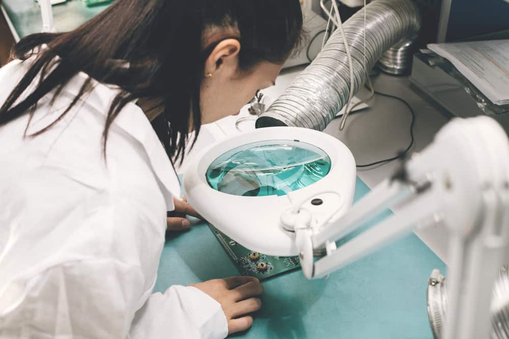
- Manual Inspection
All CMs manually inspect boards to identify obvious defects. A magnifier is often used for this test, and it is effective for discovering major surface errors.
- Automated Optical Inspection (AOI)
Virtually all CMs also implement AOI. This technique, which compares a stored image of the board created from the design files with the physical board, is an advanced version of manual inspection and will generally catch any surface error—for example, footprint pad-component misalignment, tombstoning, etc.
- X-ray Inspection
The use of X-ray technology allows for inspection below the surface of the board. This is essential for evaluating solder joints for QFNs, BGAs, and other components with underside connections. Additionally, vias on internal layers can be checked, which makes this technique applicable to fabrication. Not all CMs routinely use this testing method as it is expensive and slows the manufacturing process. Yet, it can be very valuable in identifying internal board errors—which cannot be corrected with rework— and unusable boards and increasing costs.
- Flying Probe Test
Flying probe is an in-circuit test (ICT) typically referred to as functional testing as actual component values can be acquired and compared with simulated results from design circuit analysis.
- Bed-of-Nail Test
Another ICT functional test is Bed-of-Nails. This test is very effective for taking specified measurements and identifying opens and shorts. However, design for testing (DFT) where test points are added to the layout is required, as is the assembly of a dedicated jig to align with those test points. Therefore, this technique adds time and cost to the assembly process. However, it allows for testing the entire board virtually (≤98%).
- ROSE Test
This test is a common one to determine ionic contamination, which must be minimal for certain boards, such as critical medical devices, etc. However, not all CMs can perform it, and a third-party testing facility is often called upon.
- Additional Tests
PCBAs may be put through additional testing regimens, for example burn-in testing,
Highly Accelerated Life Test (HALT), or Highly Accelerated Stress Screen (HASS), to assess performance or reliability outside of normal operating conditions. Typically, these are only utilized for boards operating in extreme environments where failure is not an option.
The first three tests listed are atypical; however, the others—although commonly known—will likely only be performed if requested.
Optimizing PCBA Quality with Augmented Reality
The most often performed PCB assembly testing methods have drawbacks—manual, AOI, X-ray, and ICT tests. The ICT tests can be expensive and time-consuming to perform, while the others are limited to surface inspection and cannot be used for functional testing. However, a new technique utilizes augmented reality (AR) overlay to combine the best of these techniques while also addressing their weaknesses. An example is shown in the figure below.
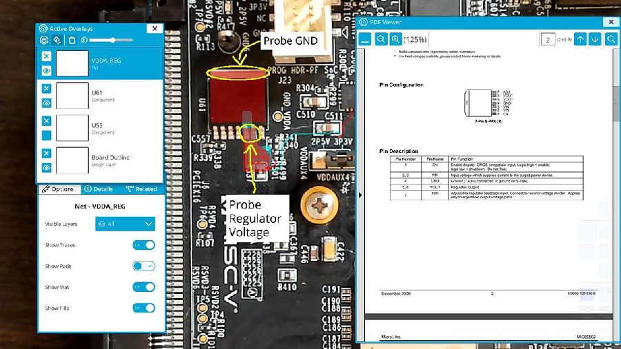
PCBA with AR overlay from InspectAR
The above figure of InspectAR, illustrates how an AR overlay can interact with a manufactured PCBA. With this technology, an engineer or manufacturing technician can compare individual components, traces, sub-circuits, or the entire board with design specifications at any point during manufacturing.
Errors can be identified easily, as with common PCB assembly testing methods. In addition, online troubleshooting and debugging can be performed to discover the best solutions before making any physical adjustments to the board through rework or the assembly process for repeated flaws. This use of software in conjunction with hardware is pointing the way to the future of PCB assembly testing and team management of ECAD.
If you’re looking for CAD models for common components, tips on the best design practices or information on advanced tools such as AR overlay for PCB assembly testing methods.
Ultra Librarian helps by compiling all your sourcing and CAD information in one place. Working with Ultra Librarian sets up your team for success to ensure streamlined and error-free design, production, and sourcing. Register today for free.


")