
PCB component footprints may appear simple, but they contain a huge amount of information required for assembly. Your PCB design application will need to take your footprints and create manufacturing documentation, such as assembly drawings and Gerber files. If your PCB footprints are incorrect or contain careless errors, you may find your board cannot be properly assembled.
Some manufacturers will not check Gerbers for pad/via errors; they simply run your board through production as long as your layout passes basic electrical DRCs. CAD programs allow you to create layouts that are electrically functional in theory, but they may not be manufacturable. To help you create accurate components, we’ve compiled a PCB footprint checklist you can use to avoid some common errors. If you’re not in the mood to create components from scratch, you can use a search service to find the CAD models you need.
A Complete PCB Footprint Checklist
When you’re creating a PCB footprint, a simple mistake might cause your board to be un-manufacturable, or it will result in a failed fabrication run. Your PCB manufacturer should check your Gerbers against your components to spot footprint, pad, and via errors, but not all manufacturers provide these services without extra expense. It’s best to keep a short PCB footprint checklist in mind when creating CAD models for your components.
Pad/hole dimensions and spacing are just two of the items you should watch for in a PCB footprint checklist. The list below shows some other important points to check when creating your PCB footprints. All these points are critical for ensuring accurate assembly with no rework.
Layer Assignment
This is placed first as it’s arguably the most important item in your checklist. Pads for SMD components obviously need to appear on the surface layer; check your settings in your PCB design software when placing pads in a CAD footprint. For through-hole components, you need to define the layer span for holes and whether the holes will be back-drilled. Back-drilling is uncommon in through-hole components unless they are placed on microwave/mmWave interconnects.
Silk screen and mechanical outlines need to be defined in their own layers. As an example, the outline for a connector might span beyond the outline of the pads or holes, and it may span beyond the edge of the component courtyard outline. This needs to be included in a mechanical layer, and it is a good idea to reflect this information in the component courtyard outline (see below).
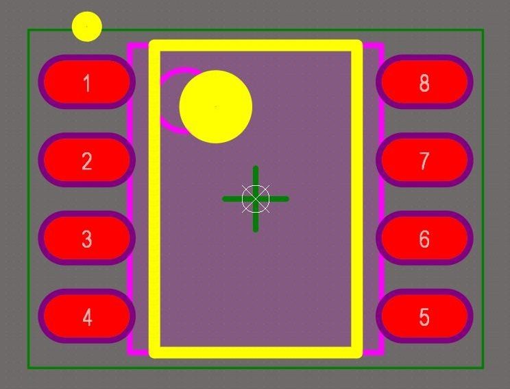
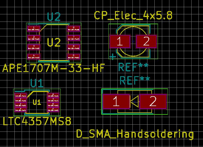
Pin 1 Indicator, Reference Designator, and Outline in the Silk Screen Layer
Aside from passives, every component has a “pin 1” that needs to be indicated in the silk screen layer. This aids assembly and ensures your components are oriented correctly. This is particularly important for components that have symmetric packaging (e.g., QFP packages and BGAs).
The silk screen layer should also include a spot for the reference designator and an outline around the component to indicate which pads belong to which components. Placing an outline around the entire component is critical for densely packed components as it can be easy to confuse pad assignments.
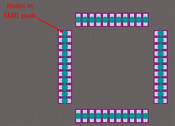
Holes in Pads
Some CAD programs will include a mounting hole in the pad by default. This will cause you to place an unused via in an SMD pad. This then causes the component to be un-solderable during assembly. Be sure to check for the presence of holes in your pad design. An example for a QFP SMD component is shown below.
Component Courtyard Outline
A component courtyard defines the minimum mechanical and electrical clearance around the edge of a component. The IPC 7351 standards define a minimum clearance area around a component edge. In the case listed above, where the mechanical outline extends beyond the pad/hole edge, the courtyard should span even beyond the edge of the component body. Your DRC utility in your PCB design software will use the courtyard outline in rules checks, so it should be included in your PCB footprint.
In terms of assembly, the courtyard edge defines a minimum clearance area around a component, which facilitates hand or automated soldering. It’s a good idea to consult your manufacturer for the appropriate component clearances for their soldering processes. Component clearance allowances depend on whether your board will be hand-assembled, or if pick-and-place assembly is used with wave soldering.
Use a Search Engine for Common Components
The PCB footprint checklist shown above can be used for any component, but you can cut down your component creation time when you use the right components search engine. Rebuilding PCB footprints for components in common packages is like reinventing the wheel, and you can cut down on your component creation time when you use the right electronic parts search engine.
The list below shows some important information you can access with the right electronic parts search engine.
- Electrical specifications: aspects like supply/output voltage, input.output current, power consumption and output, signalling standards, and other important specifications can be seen in the component description.
- Ideal applications: component descriptions might include an application or function for the component, allowing you to do an application-based search.
- SMD vs. through-hole mounting: if you’re looking for specific mounting styles, you can quickly identify through-hole or SMD mounting for different components.
- Datasheets: datasheets and mechanical drawings should be available directly from manufacturers.
- Sourcing information: you can component stocks, prices, lead times, and distributor information should be aggregated in one place.
- 2D and 3D CAD models: you can find schematic symbols and 2D and 3D CAD models in vendor-neutral and vendor-specific formats.
If you need to create CAD models for proprietary or specialty components, be sure to follow the PCB footprint checklist presented here. For other components, the parts search features in Ultra Librarian allow you to search by keyword, application, or specification. You can easily filter down to a short list of candidate parts and access CAD models for your new board. All component models can be imported into popular ECAD applications, and you’ll have access to sourcing information from worldwide distributors.
If you’re looking for CAD models for common components, Ultra Librarian helps by compiling all your sourcing and CAD information in one place. Working with Ultra Librarian sets up your team for success to ensure any design is going through production and validation with accurate models and footprints to work from. Register today!


")
")