Your component courtyards are a useful tool for ensuring components have sufficient space between them. This is a critical part of design and assembly; you need to make sure your components have enough space such that they can be hand assembled, arranged with a pick-and-place machine, or wave soldered. Your courtyard information can be easily defined in your PCB CAD tools as you create footprints.
If you’re using manufacturer-provided PCB footprints and you’re not creating your component footprints manually, you’ll have to rely on your component courtyard information being complete and accurate. As part of component courtyard management, designers need access to component models that include industry-compliant courtyard information. When you have access to the verified component footprint and courtyard data, you can rest assured your design will be manufacturable at scale. Here’s how a component data aggregator can help you find the right PCB footprints.
What is a Component Courtyard?
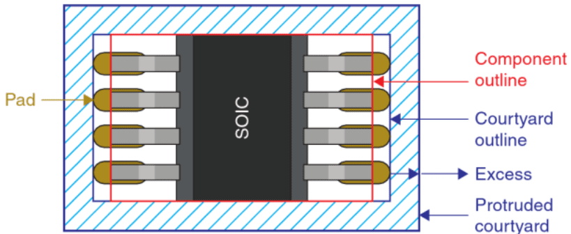
A component courtyard is the smallest area that provides the minimum electrical and mechanical clearance (called the courtyard excess) around a combined component body and land pattern. The IPC 7351 standards define requirements on component courtyard clearances. Under this standard, the courtyard sets a lower limit on clearance area around a component footprint, although there may be some manufacturing allowances that are not part of the standard. These allowances depend on the assembly process, e.g., hand assembly or pick-and-place assembly with wave soldering.
Component courtyards are one of the tools you can use in your PCB design software to ensure you’re not placing components too close together. You can also define clearances between pads as design rules, which can then be checked individually or in batches using standard DRCs. When editing a component footprint, your courtyard area should sit just outside the edge of the component, as shown in the image below. You can then select whether courtyard boundaries or pad clearance rules should be enforced as design rules in your PCB layout tools.
Component Courtyard Management Tips
Some designers will opt to use pad-to-pad and pad-to-trace design rules to define component clearances, but some components require the use of courtyards to ensure assembly. If you’re unsure whether you need components with courtyards or how to use them, keep these important recommendations in mind.
Talk to Your Manufacturer Early
Before beginning any new design, it’s important to talk with a manufacturer early to understand the limits on their fabrication and assembly capabilities. In some cases, such as when working with HDI boards, you may find that you need to consult with a more advanced manufacturer that can accommodate your design choices.
When you understand your manufacturer’s capabilities early, you’ll know when it is appropriate to violate the IPC 7351 requirements on courtyard clearances. The official IPC guidelines are based on very conservative values, but you may be able to use smaller courtyards if your manufacturer’s capabilities allow.
Understand Your Design Software
It’s important to note courtyard information may be created in some design software automatically. This can happen when defining component footprints manually, using a footprint generator, or reusing a PCB footprint that doesn’t include a courtyard.
Another important part of using your design software for component courtyard management is assigning courtyards to particular layers. This is quite useful as it allows you to choose which component clearances should be enforced using courtyards, and which should be enforced using pad-to-pad and pad-to-trace clearances.
Don’t Be Afraid to Draw Courtyard Outlines on Silkscreen
A component courtyard might sound like a component outline on the silkscreen layer, but these are not always the same thing. A component courtyard is a concept used in your design software to ensure your board complies with DFM requirements. As a designer, whether you want to include courtyards as silkscreen is your choice. Manufacturers will sometimes include them regardless in order to aid assembly.
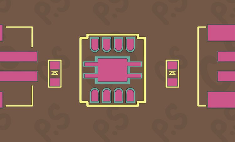
Courtyard boundaries are often placed on the silkscreen layer when component arrangements can appear ambiguous and there is insufficient room for all reference designators. Imagine a long line of SMD resistors oriented end-to-end, as shown in the figure below. If the courtyard is not drawn on the silkscreen layer, there is risk a component may be accidentally rotated during assembly. Placing the courtyard outline directly on the silkscreen layer helps ensure these resistors are placed on the correct pads and with the correct orientation, thus eliminating rework.

Only Use Verified Component Footprints
Components are only as accurate as the footprints used to define them. If your footprints are incorrect or were improperly prepared from component datasheets, then you create a risk that your courtyards are incorrect. The last thing your assembler needs is to find out your board can’t be properly assembled due to incorrectly-sized courtyard boundaries. Similarly, if courtyard outlines are not present in your component models, you may place components too close together for reliable assembly.
When you have access to verified component data directly from manufacturers, you’ll know your footprints are correct and will be compatible with your design software. You can then easily define courtyard rules in your design software, as well as place a component courtyard outline on the silkscreen layer if necessary. This goes a long way to preventing rework during assembly.
After considering these recommendations for maintaining accurate and reliable footprint information to ensure component courtyard management, the next step is simple: choose the service to acquire your PCB footprint information from.
Get the Component Data You Need for Your Next Design
Successful component courtyard management is all about ensuring your PCB footprint information is correct and that your design tools can take advantage of courtyard information in your design rule. Not all component models will include courtyard information in PCB footprints for a number of reasons. Some examples include component footprints created for HDI designs and high voltage boards. If you know you’ll be using courtyards to define component clearances, then you need access to a service that has verified 2D and 3D component models for your parts.
A parts aggregator service like Ultra Librarian gives you immediate access to a range of verified component models direct from manufacturers. These verified components include the information you need for component courtyard management, as well as sourcing information from worldwide distributors. These models can be immediately imported into popular ECAD applications.
Footprint creation and manually creating design libraries takes most teams dedicated resources and time, Ultra Librarian helps by making this process redundant especially considering component courtyards. Working with Ultra Librarian sets up your team for success to ensure any design is going through production and validation with accurate models and footprints to work from. Register today for free!