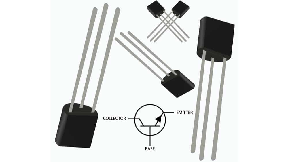
The 2N3904 is a N-type BJT and is available in the TO-92 package.
A small signal transistor is designed for low voltages and currents, not for power amplifiers. The 2N3904, registered by Motorola in the mid-1960s, is a small signal transistor used for general-purpose switching (100 mA) and amplification (100 MHz) applications. It is an NPN BJT transistor, yet it is also available in a PNP configuration (2N3906). Knowing how to read the 2N3904 datasheet, which includes the common symbols for both configurations, helps engineers better design for reliable amplification and switching applications.
Features of the 2N3904 Transistor and Alternatives
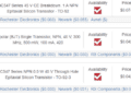
The 2N3904 transistor is one of a series that includes both NPN and PNP alternatives for various gain conditions. In today’s volatile component availability environment, these provide comparable options to improve supply chain resilience when using this device. Collectively, these devices provide a good range of general bipolar junction transistor (BJT) options for your design.
The information above is the best place to start when considering the 2N3904 transistor for your application. However, your primary resource for detailed information should be the component datasheet.
2N3904 Datasheet Transistor Specifications
The 2N3904 datasheet includes all pertinent component specifications needed to determine if the device, including alternatives, will meet your performance requirements. These include maximum ratings, transistor gain, small signal characteristics, and switching data.
Maximum Ratings
The 2N3904 transistor has maximum ratings, as shown in the table below.
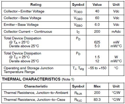
2N3904 transistor maximum electrical and thermal ratings
As you can see, the transistor can conduct a maximum of 200 mAdc with a maximum applied input voltage of 6 Vdc between the base and emitter. However, the device is unsuitable for high-power applications (as shown by the milliwatt-level power dissipation).
Transistor Gain
The table below shows the ON characteristics of 2N3904.
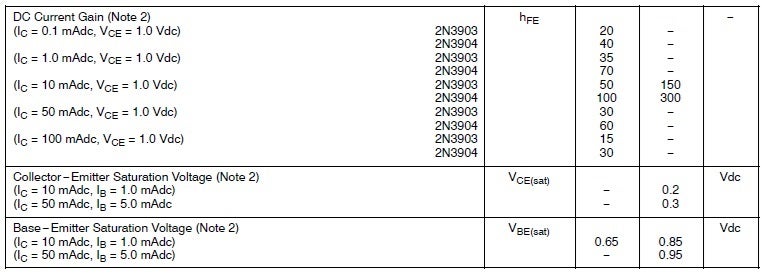
Transistor gain for the 2N3904 and alternatives
The 2N3904 datasheet lists the DC gain (hFE) of its alternative 2N3903 (PNP) in separate rows. You can see that the PNP type has 50% less gain than the NPN type, which is the biggest reason why the NPN type is so popular. The minimum gain for 2N3904 is 40 for IC = 0.1 mA, which goes up to a maximum 300 for IC = 10 mAdc at VCE = 1.0 Vdc. At this point, the gain is ten times the minimum that the transistor gradually achieves at the end for IC = 100 mAdc at VCE = 1.0 Vdc.
This analysis acknowledges the importance of designing the transistor’s circuit for hassle-free operation despite a high gain bandwidth.
The maximum voltage drop across the device (Vce) during the ON condition can have two different values as follows:
- 0.2Vdc when the IC = 10 mA and a 1 mA current on the base (hFE = 10)
- 0.3Vdc when the IC = 50 mA and a 5 mA current on the base (hFE = 10)
Small Signal Characteristics
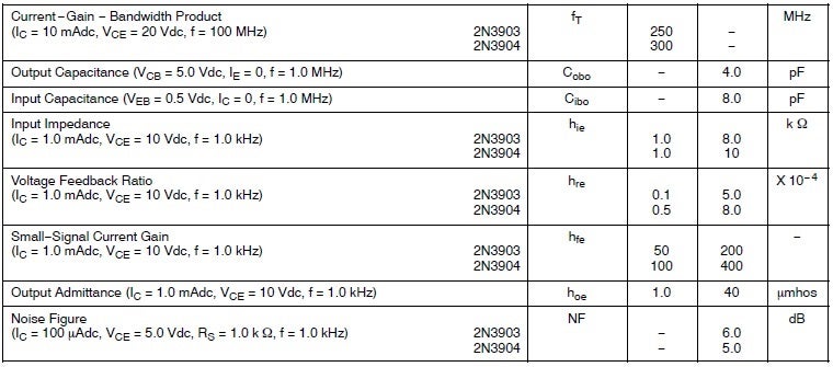
Small signal characteristics for the 2N3904 transistor
The term fT represents the frequency at which the output signal current will be equivalent to or less than the input signal current, irrespective of the set amplification. That means, at this frequency, the transistor can no longer amplify the signal.
The term NF represents the internally generated noise by the transistor due to temperature fluctuation, which should be no worse than 5 dB in this case, as per the 2N3904 datasheet. If your application is sensitive to this much noise, e.g., RF amplifiers, and requires an extremely quiet device, transistors like 2SC3324 or 2N5088 would be your ideal bet.
Switching Characteristics
Due to the transistor’s inherent capacitance (Cce, Ccb, Ceb), the current rises and falls over time. It’s not instantaneous, as the capacitor takes some time to discharge.
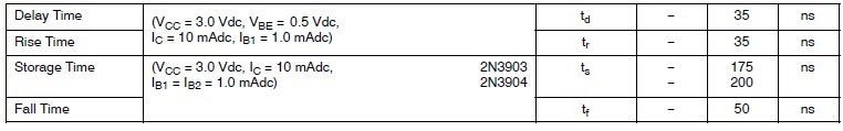
2N3904 switching characteristics
As per the 2N3904 datasheet, the transistor takes 35ns to rise from its initial value to 10 % of its final value (delay time) and the same time to reach 90% of its final value (rise time). The storage time indicates the time required to get the carriers out of the base of the transistors.
Applications of the 2N3904
The 2N3904 excels in the following circuit operations:
- Minimum load switches (up to 200mA) for less saturation voltage and maximum gain
- Amplifier modules, such as audio amplifiers and signal amplifiers, are used because of their high current gain
- Automatic-switching applications
- Fast-switching applications such as pulse width modulation
- Home appliances such as TVs and stereo systems
Packaging and Dimensions
The transistor is available in through-hole and SMD packages, TO-92, shown below, and SOT-23 and SOT-223, respectively.
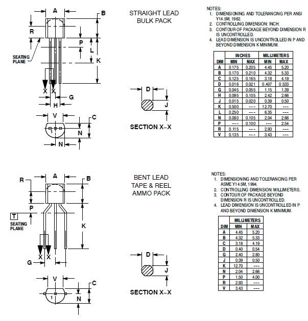
Packaging options for the 2N3904 transistor and alternatives
PCB Design with the 2N3904
The 2N3904 datasheet should be your primary resource for evaluating the viability of using the component and for your design after selection. In addition to critical specifications and packaging options, the datasheet also includes performance graphs, such as the characteristics below.
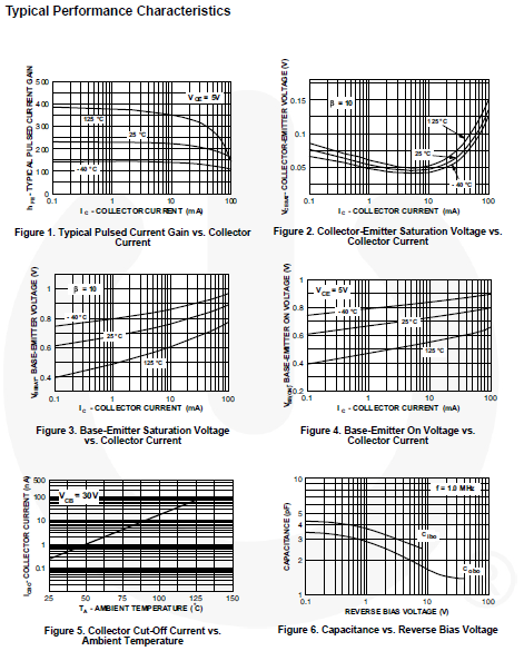
2N3904 performance characteristics
The datasheet also provides information for creating footprints and landing patterns. It is not recommended to attempt to create these manually, as any flaws will be costly. Increased development time, additional manufacturing costs, and even redesign are possible when CAD models are not accurate. The best option is to rely on the industry leader in creating and supplying manufacturer-vetted and industry-standard compliant CAD models, Ultra Librarian. This includes the 2N3904 below.
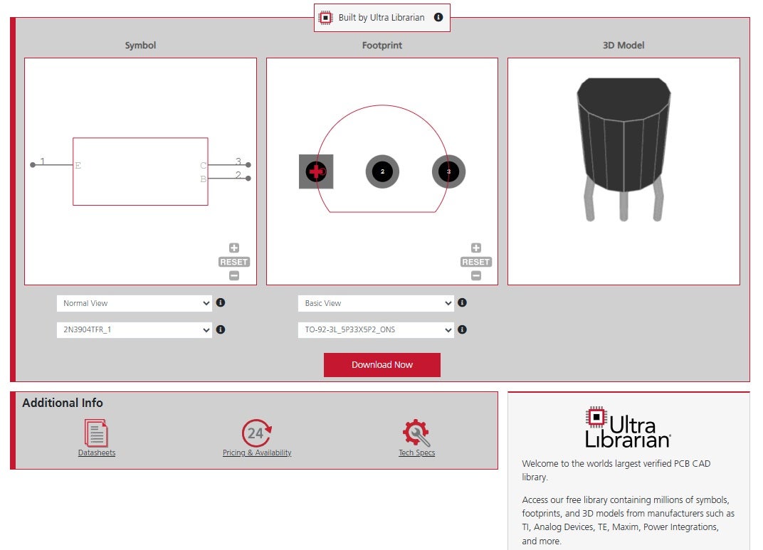
2N3904 schematic symbol, footprint and 3D CAD models from UL
If you’re looking for CAD models for common components or important design information on how to best use the 2N3904 datasheet for your project, Ultra Librarian helps by compiling all your sourcing and CAD information in one place.
Working with Ultra Librarian sets up your team for success to ensure streamlined and error-free design, production, and sourcing. Register today for free.