Every PCB will need to pass through a soldering process for efficient assembly. Designers don’t need to know all the ins and outs of every PCB soldering technique, but they should make sure they design footprints correctly to ensure low defect rates during assembly and prevent rework. Before you start designing your own footprints, take a look at datasheets and understand PCB soldering processes to ensure accurate assembly.
PCB Soldering Techniques and Processes
PCB assembly houses are responsible for selecting the right processes to solder and assemble your board with the goal of ensuring zero defects and rework. Assembly shops have to match up the process they’ll use for assembly with your set of components, which can be more difficult than it sounds. Boards that have a complex mix of SMDs, through-hole components, and multiple BGAs on a double layer board will require a more complex process than a simple single-sided board with a single mounting style and reflow profile.
You might also consider soldering your own boards by hand, especially if something is a one-off design and you don’t feel like paying for automated assembly. Moderate volume runs will sometimes use hand soldering, so this process is not limited to makers or hobbyists. Automated PCB soldering processes include wave soldering, hand soldering, and selective soldering.
Wave Soldering
Wave soldering is normally used with through-hole components, although it can also be used with surface-mount components, such as larger integrated circuits, as long as they are placed correctly along the conveyor path. In wave soldering, a PCBA is placed on a conveyor that passes the board through a “wave” of molten solder created by a pump. This coats the exposed metal on the board with molten solder, which then hardens and forms a joint along the component lead.
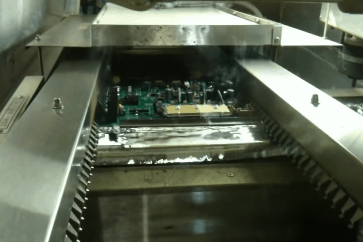
A PCB passing through a wave soldering machine
Reflow Soldering
The standard process for assembling SMD components is reflow soldering. In this PCB soldering technique, a solder paste is used to temporarily attach components to their pads, and the PCBA is slowly heated up to a final temperature (typically about 200 °C). This brings the solder paste into a molten state, where it then begins to flow and form a joint between component pins and landing pads. As the solder cools, it solidifies and forms a strong eutectic. Before passing through a reflow oven, solder paste is applied with an automated CNC system.
Selective Soldering
Selective soldering is the automated analogue of hand soldering. This CNC process involves scanning a soldering iron and a solder nozzle across a board, and molten solder is selectively applied to each lead. The amount of solder and heating time can be controlled during programming, which helps prevent cold joints. This process is sometimes used as an alternative to wave soldering or hand soldering. If it is difficult to apply solder to certain leads on a component (such as bulky through-hole connectors), and if a large number of these components are involved, then selective soldering will be a useful alternative to hand and wave soldering processes.
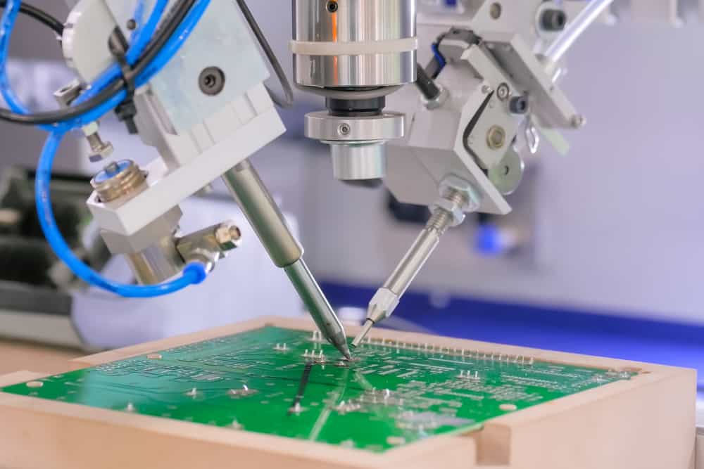
Selective soldering process
Variants of selective soldering involve selective reflow, where solder paste is selectively applied to specific components and the components are reflowed. Selective wave soldering is another option, where a solder flux is selectively applied to through-hole component leads and the board is placed into wave soldering. A mask can also be used in selective wave soldering to limit where solder is applied. Finally, there is laser soldering, where a high-intensity laser beam is used to melt an alloy and form a solder joint.
The table below summarizes these three primary PCB soldering techniques and which components normally require them.
| Process | Component types |
| Wave soldering | Normally used with through-hole components, can be used with SMD components. |
| Reflow soldering | Normally used with SMD components. |
| Selective soldering | Used for through-hole components on PCBAs that also contain reflowed SMD components. |
Hand Soldering
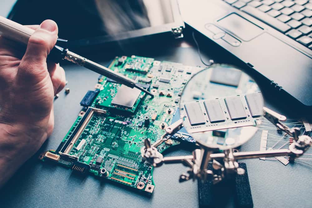
Soldering your components by hand is fine if you’re working on your own board and you don’t want to pay a shop for automated assembly. Larger components like axial through-hole resistors and some larger SMDs can be soldered by hand. Once you’re dealing with denser packaging, such as fine-pitch QFN packages and 0603 or smaller SMD passives, the risk of bridging or insufficient solder increases, especially when using wire with a soldering iron.
These components need to be large compared to your soldering iron to make sure you don’t accidentally bridge leads between densely packed components. Some engineering of the land pattern and footprint may be required to ensure you’ll prevent bridging or weak joints.
Footprints, Land Patterns, and Soldering
Footprints and land patterns that are designed to comply with IPC standards are constructed to account for standard soldering processes (reflow or wave). IPC standards also define acceptance criteria for solder fillets, and land patterns are constructed so that standard processing can meet these criteria. It’s sometimes difficult to meet these criteria in hand soldering, so automated equipment is used to ensure higher quality.
To help ensure quality in automated processes, make sure you follow your component datasheets when you need to create PCB footprints. Component manufacturers do a great job of following standards and testing PCB solder processes with their components, so make sure you follow their footprint guidelines. Another option to ensure your footprints are correct is to use manufacturer-supplied footprints through an electronics search engine. These footprints are validated to ensure they are accurate and will comply with industry standards to ensure accurate assembly.
When you need to find electrical data and ECAD models for different types of PCBs that are verified by component manufacturers, try using the electronics search engine features in Ultra Librarian.
Working with Ultra Librarian sets up your team for success to ensure streamlined and error-free design, production, and sourcing. Register today for free.