KNOWLEDGE OF PCB ASSEMBLY TERMINOLOGY HELPS YOU BUILD SUCCESSFULLY
Just like ECAD software and PCB fabrication, the processes used in final PCB assembly have their own vocabulary. In addition, there are many peculiarities in standard PCB assembly processes that influence design decisions. If the board is designed to accurately accommodate standard PCB assembly processes, you can ensure high yield with little to no rework.
Unfortunately, ECAD software vendors don’t always do the best job of communicating the important aspects of PCB assembly to their users. Additionally, fabricators will inspect for DFM concerns, but not for assembly concerns. It’s up to the astute designer to ensure their boards can be produced without assembly defects, and it starts by understanding important PCB assembly terminology.
GLOSSARY
The glossary shown here is divided up into three sections—general terminology used to describe PCB assembly equipment and processes, soldering terminology, and inspection and testing terminology as part of quality control.
General PCB Assembly
PCB Soldering
Inspecting & Testing
General PCB Assembly
GENERAL PCB ASSEMBLY TERMINOLOGY
PCB assembly (PCBA) (noun)
The name given to a fully assembled printed circuit board. This is sometimes used interchangeably with printed circuit board (PCB). The former refers to fully assembled products, while the latter refers only to bare circuit boards before assembly.
PWB assembly
A printed wiring board (PWB) assembly is an older term that is synonymous with PCBA.
Bill of materials (BOM)
The list of components, their quantities, their sourcing data, and reference designators on the PCBA.
Do not populate (DNP)
A designation given to some components on a BOM, indicating that the specific components should not be placed on the PCBA.
Pick and place machine and SMT feeder
An automated assembly machine that pulls components from packaging and places them on the circuit board in the correct location. An SMT feeder pulls components into the pick-and-place machine so that they can be soldered.
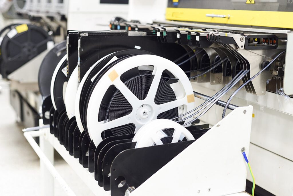
Tape-and-reel
A method of packaging SMT components so that they can be quickly pulled into a pick-and-place machine with an SMT feeder for automated placement on the bare circuit board.
Components in tape-and-real packaging are being fed into a pick-and-place machine with an SMT feeder
Aperture
The hole at the end of a vacuum nozzle used in pick-and-place machines. The vacuum is used to pull SMT components from the SMT feeder and drop them onto the board in the appropriate spots. Smaller package sizes will require smaller apertures.
Depaneling
Removal of a finished PCBA from its assembly panel. This can be done with CNC routing, by cutting along a scored V-groove, or by snapping breakaway rails from around the board edge.
Component kitting
Refers to the process of supplying a production-ready kit or batch of electronic components.
Underfill
A liquid polymer material that is applied to a PCBA after it has passed through reflow. The underfill covers the underside of integrated circuits and other components to provide extra protection.
Conformal coating
A transparent coating that can be applied to a PCBA by spraying. These coatings provide environmental protection and can even function as an absorber for high-frequency EMI.
Burn-in testing
A pre-assembly test, where components are operated at elevated temperatures to simulate excessive stress. This allows premature component failures to be detected before they are placed in a PCBA.
PCB Soldering
PCB SOLDERING TERMINOLOGY
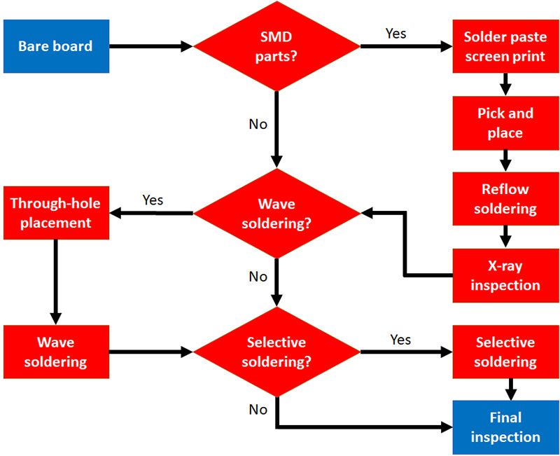
Soldering is the process by which components are attached and secured to a bare board during PCB assembly, and it is one of the greatest determinants of product quality and lifetime. Soldering follows two different processes, depending on whether SMT or through-hole components are used in the PCBA. The flowchart below shows the progression through the PCB assembly process and how soldering is involved for each type of component.
Copper pour, traces, vias, and reference designators in a KiCAD PCB layout.
Solder joint
The metal fillet that connects a metal lead on a PCB component to its landing pad (for SMD parts) or its mounting hole (for through-hole parts).
Wave soldering
A bulk soldering process where through-hole components are placed on a board with solder flux, and the board is passed over a pan of molten solder. A vacuum pump produces a “wave” of molten solder that passes over the board and coats the board. Controlled cooling then produces the desired solder joint.
Reflow soldering
The process used for soldering SMD components during PCB assembly. Reflow soldering uses a solder paste to ensure solder attaches only to desired copper areas. Controlled heat is used to melt solder and form a solder joint.
Solder paste
A mixture of solder flux and powdered solder that melts to form the solder joint during reflow soldering.
Fun Fact
Soldering of SMD components is predominantly done with reflow soldering, but wave soldering can also be used for high-throughput assembly.
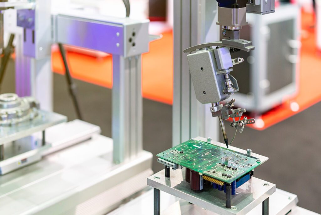
Selective soldering
An automated alternative to hand soldering, where a CNC machine moves a soldering head around the board and solder is applied to through-hole components.
Selective soldering being used to assemble through-hole components
Laser soldering
Another alternative to hand soldering and selective soldering, where a high-power pulse laser is used to melt solder and create solder joints.
Types of solder
Different types of solder are distinguished by their tin content and other alloying metals. Tin-lead is the common solder with common Pb:Sn ratios of 60/40, 63/37, 50/50, 30/70, and 10/90. Another common mixture is 62/36/2 (Sn/Pb/Ag).
LTS solder
A type of solder that can be used at a lower temperature than other types of solders. An example of a Pb-free LTS solder is Sn-Bi, although some tin-lead solders can qualify as LTS solders.
Pb-free solder
Solder alloys that do not contain any lead (Pb). These solders are used to comply with Restriction of Hazardous Substances (RoHS) regulatory requirements in the EU.
Solder flux
A chemical agent that performs multiple functions during soldering. Flux protects the metal surfaces from re-oxidation and allows molten solder to easily flow by altering the surface tension of molten solder. Leftover solder flux needs to be thoroughly cleaned after assembly.
Fun Fact
Solder flux comes in three varieties, each of which requires different cleaning processes and solvents:
Rosin-based fluxes will need to be cleaned with specific solvents that are typically fluorocarbon-based.
Water-soluble fluxes can be cleaned with deionized water and detergents.
No-clean fluxes claim to require little or no cleaning, but the residual no-clean flux can reduce the adhesion strength of any conformal coatings.
Keep these points in mind when planning for high-throughput, low-cost assembly.
Inspecting & Testing
INSPECTION AND TESTING TERMINOLOGY
Once a board has passed through soldering, it is ready for inspection and final testing. Here is a short list of important inspection and testing processes used to evaluate PCBAs and ensure high yield.
Automated optical inspection (AOI)
A computer vision machine that automatically inspects the surface of the board for catastrophic failures and quality defects.
X-ray inspection
Complex components with hidden solder joints, like BGAs or LGAs, can be examined with X-ray inspection. This form of non-destructive testing allows shorts, opens, or cracked solder joints to be identified.
Automatic test equipment (AQE)
Generally refers to any test equipment that can automatically inspect and gather measurements from a PCB/PCBA.
In-circuit testing
An automated test where electrical probes are used to check for shorts and opens, resistance, capacitance, and other electrical quantities on a PCBA. The results can show whether the assembly process produced some defect.
Continuity testing
Performed during in-circuit testing, this is intended to locate the presence of open or short circuits in certain nets on the PCBA.
Bed-of-nails tester
An AQE machine that is used for automated in-circuit testing. In this tester, electrical probes are placed in fixed positions and are brought into contact with test points on the PCBA.
Flying probe tester
A faster machine used for automated in-circuit and bare-board testing. In this machine, test probes are automatically moved around the PCB to make contact with various test points and gather measurements.
FIND PART DATA WITH ULTRA LIBRARIAN'S ELECTRONICS SEARCH ENGINE
At Ultra Librarian, we care deeply about the success of all PCB designers and engineers, and we strive to provide resources to help new designers advance their careers. In addition to our glossaries with PCB assembly terminology, we provide a comprehensive electronics search engine that helps designers find the components they need. All Ultra Librarian users can access CAD models for components and verified 3D models that can be imported into popular ECAD applications. We also give users access to aggregated sourcing information from worldwide distributors.