Designing circuit boards has to be one of the most exciting careers that anyone could embark upon. That is especially true today, as our world is becoming more and more reliant upon electronics for everything from domestic chores–such as washing dishes and vacuuming floors–to transporting us to wherever we need to go–through automatic train track switching and auto-piloting airplanes. And the future will likely be full of even more amazing board designs that will comprise electronics products that cannot be imagined today.
Yet, no matter how great a design may seem to be, it must be built in order for us to reap the intended benefits of its application. Therefore, along with a boundless imagination and creativity, PCB designers must also follow well-defined guidelines and rules and to ensure operation and that their design can be fabricated and assembled. This includes following PCB layout best practices for manufacturability.
PCB Layout Best Practices to Ensure Manufacturability
Regardless of whether your project is for a new custom design or an improvement upon an existing one, a primary objective is to have your board built as efficiently as possible. Doing so reduces turnaround time, optimizes resource utilization, and lowers costs. The best way to meet this objective is by knowing and following PCB layout best practices for manufacturability, as listed below.
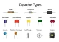
Choose the right materials for your board type
It is far too common when designing boards that software defaults are accepted without considering if these options actually are the best for the specific PCB being developed. The choice of board material is probably the most common example of this. Although FR-4 is a good general choice, it is not always the most appropriate selection. For example, if the board will be exposed to high temperatures, lower glass transition temperature (TG) rated boards may be subject to deformation or premature breakdown.
Acquire and follow your CM’s DFM rules and guidelines
Without a doubt, the overriding best practice when designing circuit boards is to acquire and follow the design for manufacturing (DFM) rules and guidelines provided by the contract manufacturer (CM) that will actually build your PCB. By following your CM’s DFM rules, you ensure that the dimensions and specifications for your PCB layout fall within the capabilities of the equipment used by your CM. Incorporating these practice will lead to higher first pass yield rates, lower manufacturing costs, and faster bring up.
Use accurate component CAD models
Component datasheets are Invaluable assets when designing your board. This is especially true for semiconductor parts like microprocessors, FPGAs, and expanders. These documents provide information about the internal operation of ICs and modules, pinouts, typical applications, and footprint and schematic symbol drawings that can be used to create these elements from scratch. For the best, most accurate symbols and footprints; however, you should rely on CAD models that have been verified with the manufacturer, which can be found online.
Prioritize SI and PI when routing traces
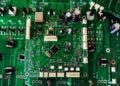
Circuit board with complicated trace routing
Obviously, routing the traces on your board is important. And these signal networks can be complex and do directly affect signal integrity (SI) and power integrity (PI). In fact, how you run the routes affects everything from where components and connectors are placed and vias are located to the electromagnetic compatibility (EMC) of your design. Therefore, following good routing tips that minimize electromagnetic interference (EMI) on your board should be the priority. These include ensuring adequate spacing, lengths, and copper weights.
Use adequate spacing/clearance between surface elements
Another important consideration when laying out your board is spacing. As virtually all elements on the board emit and/or receive energy at some level, adequate spacing is required to minimize interference or reduce noise along signal paths. Moreover, creepage, stray capacitance, and arc tracking may also become significant where there is inadequate spacing between elements.
Leave adequate board edge clearance
In addition to spacing between board elements, it is also critical that the spacing between elements and the board edge is sufficient, as well. Although the effects of not following this practice are felt primarily during post-assembly, not leaving enough board edge clearance can result in respins, which includes fabrication.
Follow good PCB stackup tips
Due to the thrusts for smaller electronic devices, board package size is often restricted. This means that multilayer boards must be used to meet the functionality and performance requirements. Typically, there are CM recommended stackup configurations and limitations on the number of layers that can be constructed. Additionally, there are signal layer and grounding rules that must be followed to achieve the best signal integrity, minimize noise, and institute good thermal dissipation.
Use the correct drill hole type and size
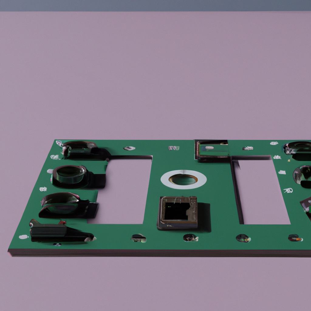
PCB with multiple drill holes
For most designs, multiple drill holes are required. These include non-plated through holes (NPTHs) and vias or plated through holes (PTHs), which are used for mounting and signal routing, respectively. Depending upon the type of drill used, there are different aspect ratio limitations. Additionally, there are standard requirements for drill hole size and aspect ratio that must be followed.
Run DRC checks often
It may seem as though running a single design rule check (DRC) once the design is completed would be sufficient. However, in practice this is rarely, if ever, the case. In most cases, you will be confronted with multiple violations that should be alleviated prior to passing your design to the CM. Therefore, the best practice is to run DRC checks in real-time. That is to use a design program with the capability to check each design step for DRC–which should include your CM’s DFM–compliance. In lieu of this, you should perform DFM checks often during the design process.
Use a CAD design file format
For the past few decades, Gerber files have been the de facto standard for PCB design files. However, the current trend is to use a CAD format, instead. The primary reasons for the change are that CAD files are more accurate, compact and inline with the formats that CMs actually use. Therefore, it is recommended that you use the preferred CAD format for the CM that will actually build your board. Additionally, 2D and 3D CAD file formats improve the ECAD-MCAD integration process.
By following the PCB layout best practices listed above, you will be able to create board designs that support the manufacturing stage of development, and minimize costs and turnaround times.
If you’re looking for CAD models for common components or important design information like the essential PCB layout best practices to know, Ultra Librarian helps by compiling all your sourcing and CAD information in one place. Working with Ultra Librarian sets up your team for success to ensure streamlined and error-free design, production, and sourcing. Register today for free.