Certification of PCB design verification
As a PCBA designer or developer, you are expected to create good designs. And, in many cases, you will not be singled out for this achievement as it is, after all, your profession. Instead, the affirmation must come from the development process itself. And, not only does it but it is required. If your creation does not pass PCB design verification criteria, it will never transition from prototyping to volume production.
PCB Design Verification vs PCB Design Validation
For new product introduction (NPI), prototyping is a critical process as this is where an initial design is converted into a final production-ready board. The prototyping process is cyclic and consists of three stages: design, build and test or D⇒B⇒T. One of the primary objectives of this process is to attain a board that can be certified or validated as meeting the operational and performance criteria for which it is intended.
| Definition
PCB design validation is the process of evaluating a circuit board design to ascertain whether it is capable of fulfilling its intended function. This is typically done by subjecting the PCBA to a test regimen whereby its electrical parameters—voltages, currents, powers—are measured at critical points and compared with the expected values. |
PCB design validation is a functional testing process usually performed by the developer, at least in part during the test stage of the cyclic prototyping process. Thus, testing is also at the root of PCB design verification.
| Definition
PCB design verification is the experimental process of ensuring that the board’s physical parameters are within acceptable ranges and tolerances as defined by PCB manufacturing standards for the performance classification level stipulated in the design. |
The performance classification level mentioned in the definition above is either class 1, class 2, or class 3 as defined in the IPC 6011 Generic Performance Standard for Printed Boards. In contrast to validation, the actual board testing for PCB design verification is done by your CM. However, verification is a collaborative exercise for the most efficient board build process that begins with design and extends through fabrication and assembly.
How Your PCBA Design Prototype is Verified
Although many PCBA manufacturers still rely on manual processing and the skills of technicians, more advanced board building is software-based and mostly automated. For the former, it is essential to sample test physical boards to ensure that parameters and design specifications meet requirements. For automated processes, inspections are still needed; however, verification relies to a great extent on ensuring that design file–or package in the case of Gerber files–specifications adhere to your CM’s DFM rules and guidelines which are set according to standards and their equipment capabilities. These specifications are then programmed into the appropriate equipment.
Irrespective of the level of automation employed by your CM, your design choices are an integral foundational aspect of the PCB design verification process.
PCBA Design Verification Process Steps
Designer
- Setup DRC
The first step in PCBA design verification is specifying the parameters of your board layout, such as clearances, drill hole locations, and sizes, etc. These should fall within your CM’s DFM rules. - Perform DRC checks during design
The best design practice is to continually run DRC checks as you make adjustments to your design. Failing to do this can make it more difficult to isolate the root cause of violations and extend the time for your design. - Perform final DRC check
After all, components have been added and traces run, including vias and inner layer routes, a final DRC check should be performed. If no violations are indicated, the design package should be prepared and sent to your CM.
Manufacturer
- Perform DFM check
Most CMs will perform an initial DFM check to ensure manufacturability before starting fabrication. Moreover, some CMs will do this evaluation before giving you a quote so that any necessary design changes can be done before initiating your board build. - Inspect board during manufacturing
As your board proceeds through the manufacturing steps, your CM will perform PCB testing. The specific inspection and testing methods used are CM dependent but will likely include visual, AOI, and optical board penetrating tests. - Perform final PCBA testing
If necessary and/or requested, your CM may test your board for structural integrity, ionic contamination, or other physical attributes.
As indicated, the best PCB design verification process is not a single activity but a collaborative effort between you and your CM. And as with the entire board development process, the best results are obtained when the best tools are utilized.
The Best Tools for PCBA Design Verification
Conventional PCB design verification tools, such as cameras and X-ray machines, are used to analyze the physical board and determine how closely it matches the ideal projected board design. These methods are effective; however, new, more advanced tools, such as augmented reality (AR) overlays, as shown in the figure below, are expanding the landscape.
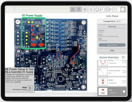
AR overlay tool for PCB design verification
In the figure above, an example of how InspectAR’s software testing package can be integrated with HW board testing is shown. This advanced tool utilizes data-driven board design, where circuit simulations are performed during design to eliminate issues that may result in faults during manufacturing and to create data that can be used for comparison during testing. These capabilities greatly improve the effectiveness and efficiency of PCB design verification, enabling you to transition to production faster and with higher yield rates.
If you’re looking for CAD models for common components or useful tips like the best PCB design verification methods and tools, Ultra Librarian helps by compiling all your sourcing and CAD information in one place.
Working with Ultra Librarian sets up your team for success to ensure streamlined and error-free design, production, and sourcing. Register today for free.