There is a lot that happens behind the scenes in a PCB manufacturing facility and one of the important processes in qualifying new boards is testing. A new PCB can go through various levels of testing and inspection, depending on the needs of your particular product. Some tests are simply DC electrical tests, where a design is inspected for continuity, and testing processes can only get more complex from there.
To ensure your design will be fully testable during and after manufacturing, there are some simple things you can do to make sure the design can be reliably probed. For more advanced designs, such as a board for a highly rugged system or an RF product, your testing requirements may be non-standard and won’t be performed by most manufacturers. Before you grab your multimeter and start testing your own boards, make sure you know what PCB testing methods and inspections your manufacturer will perform.
Standard PCB Testing Methods and Processes
During manufacturing, a fabricator and/or assembler will perform three possible groups of tests to evaluate your board’s electrical characteristics. These PCB testing methods focus on electrical behavior and lifetime, and different tests are needed for different systems and production volumes.
In-Circuit Testing
This test is intended to check for opens or shorts in a fabricated board before it is placed into assembly. This is done using a flying probe machine, which quickly moves probes between different points on a board to check for continuity. The other method used for in-circuit testing before assembly is a bed of nails test. Both types of pre-assembly in-circuit testing are used to verify net connectivity and to ensure that the open/short measurements in the fabricated board match data in the PCB netlist.
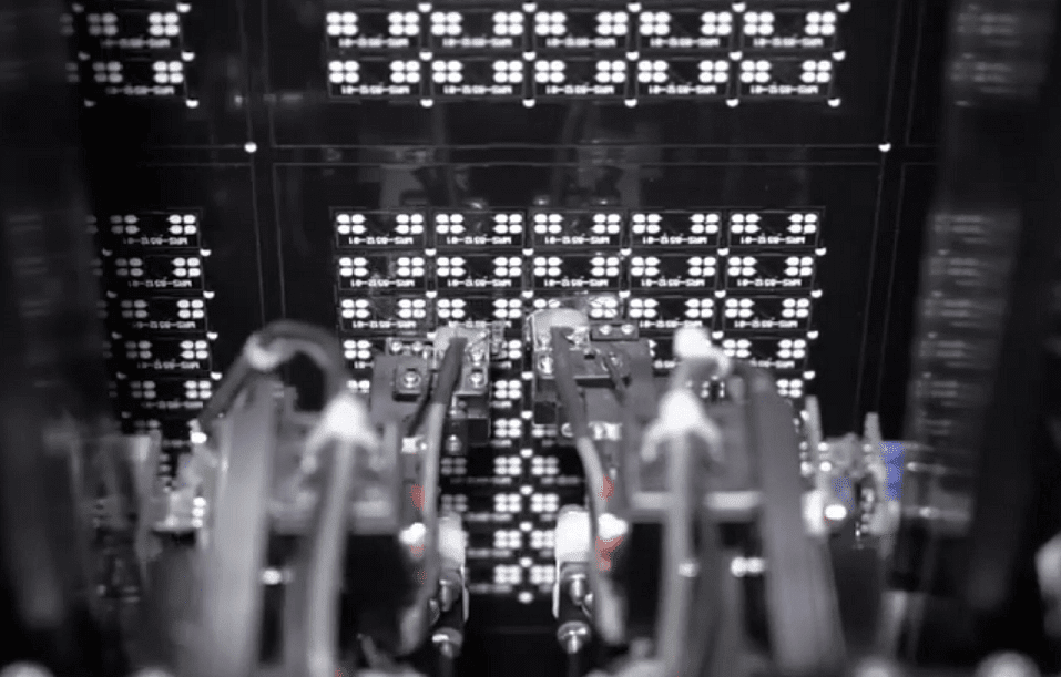
Live in-circuit test with a flying probe machine
In-circuit testing is also used to test PCBAs and gather specific electrical measurements. Examples include measuring regulator power output, specific AC waveforms with an oscilloscope, or TDR measurements. This level of testing is normally performed at a higher volume, as it can carry a higher NRE charge, making it less economical for low-volume production runs. At some point, a designer may want to consider outsourcing their functional testing to ensure the design meets performance requirements.
Functional Testing
Functional tests go beyond electrical testing during board fabrication and assembly. They largely verify whether a PCBA can provide the desired user experience as well as whether it can meet some basic requirements the board will encounter in the field. These tests can be used to assess firmware/software functionality, the behavior of peripherals (motors, switches, etc.), user interfaces, and the overall link between all of these in the design. Your manufacturer isn’t doing these tests to help you as part of the design process; they are verifying the as-produced board can support the minimum required functionality in your product.
Not all manufacturers are equipped to provide this level of testing, as it can involve multiple time-consuming manual tests by human operators, which bring additional costs. These boards also need to be specifically designed to support functional testing by a fabricator, sometimes with specific test fixtures and custom firmware/software. For this reason, automated aspects of functional testing are sometimes performed by a prototyping house, and the end customer will perform field tests with the prototyped board. Once a design passes these tests, automated tests for electrical and functional behavior are implemented on the production line.
Burn-In Testing
Burn-in testing is a form of accelerated life testing. The purpose is not to simulate overly stressful conditions, but rather simulate degradation in integrated circuits and other components by operating these devices at high temperature. Once a batch of boards is assembled and deemed operational, the batch can be placed in a heated oven while powered and operating; typical burn-in times range from 48 to over 150 hours. The least reliable boards will fail first (called “infant mortality” failures) and are removed from the batch. These failed boards can be inspected further to identify the primary failure points and propose redesigns to be applied in the next revision.
The table below shows a short summary of these three standard testing methods, their advantages, and disadvantages.
| PCB Testing Method |
Advantages | Disadvantages |
| In-Circuit Testing |
Locates all the major quality defects associated with fabrication as well as some assembly defects | Development is expensive, either through costly programming (flying probe) or fixture placement (bed of nails) |
| Functional Testing |
Identifies problems with interfaces, user experience, software/firmware, and mechanical design that can’t be identified in other tests | Requires standardized testing procedures be compiled and given to assemblers, may require custom programming |
| Burn-In Testing
|
Eliminates early failures from production runs, proves reliability as required in some industry standards (MIL-STD, etc.) | Only useful in high-volume runs where enough data can be gathered to make meaningful statistical conclusions about quality, costly due to scrapped components and boards |
Non-Standard Mechanical and Electrical Tests
There are many other tests that are non-standard or are not generally performed by PCB manufacturers. Once you receive your PCBA, you’ll be responsible for commissioning any other required tests that aren’t performed by your manufacturer. If you need to perform more specialized testing, there are external labs that can provide these services, or they can be performed in-house. Some non-standard PCB testing methods include:
- Vibration and mechanical shock testing
- Thermal cycling testing
- ESD testing
- Signal integrity and power integrity testing
The final point above is particularly important early in the design, as it requires placing test fixtures on the board so high-speed channels can be accessed for measurements after assembly. A typical test fixture is an SMA connector, which is available in horizontal and vertical configurations. When you need to place a test fixture on your board, make sure you have access to the correct footprints for your components.
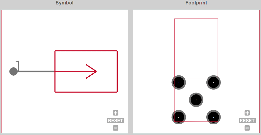
Schematic symbol and PCB footprint for Molex 73100-0114
When you need to find electrical data and ECAD models for fixtures used in PCB testing methods, try using the electronics search engine features in Ultra Librarian. All ECAD data you’ll find on Ultra Librarian is compatible with popular ECAD applications and will help you streamline your design process. You’ll also find datasheets and sourcing information from major distributors.
Working with Ultra Librarian sets up your team for success to ensure streamlined and error-free design, production, and sourcing. Register today for free.


")