
PCB footprint creation ensures components solder down correctly during assembly.
Before proceeding with the layout, designers must create the footprints that act as the interface between the PCB and its components. While PCB footprint creation can be a relatively simple procedure in the grand scheme of ECAD, a small mistake can lead to significant manufacturing or performance issues. Correcting these faults may require a design revision that can hamper budgets and project turnaround times. A strong organizational focus on footprint creation will standardize this approach.
Beginning PCB Footprint Creation
PCB footprint creation always starts with the manufacturer’s datasheet (or similar documentation) that details the physical dimensioning of the parts. There are two primary methods for creating new footprints:
- Users can pick from various footprint wizard tools for components that are “IPC standard” (i.e., common package styles like SOIC, PDIP, DPAK, BGA, etc.). These tools simplify PCB footprint creation to the essential dimensions of the package (body length/width, pin length/width/pitch, etc.) for ease of input.
- Alternatively, users can design the footprint more meticulously in their ECAD environment of choice. Instead of inputting the various parameters, users will create the shapes and assign layers manually. While this process is more time-intensive, it is also far more customizable than the wizard tools. Manual creation trumps wizard tools for many components that don’t fit neatly into a package designation.
Designers should also be aware of footprint reuse. Some footprints may be similar to a standard package type with a slightly different pinout (extra/missing pins, changes to (a) pin dimension(s), etc.); these components are an excellent opportunity for librarians to reconfigure a verified footprint. There are numerous benefits to this approach:
Benefits of using Standard Package Footprints
- Using verified footprints as a springboard for a new design means the new footprint has a much smaller chance of error, as less “new” content is generated.
- Assuming the organization uses standard IPC naming conventions for footprints, it’s trivial to look up the closest package, copy the footprint, and edit the footprint/name as necessary.
- Verifying these repurposed footprints can be exceedingly expeditious if the naming convention follows IPC, as any changes from the original are reflected in the name (changes to body dimensions, pin count, pitch, etc.)
Steps for Ongoing Library Maintenance
Ultimately, PCB footprint creation coalesces into a PCB library, where maintenance is necessary to ease navigation and prevent footprint duplication that can undermine the verification process.
- All footprints within the library should have the same layers, orientation, model attachment (e.g., STEP), and naming convention. Consistency is critical to ensuring the library’s usefulness.
- When looking through datasheets, it’s essential to understand the component beyond the pinout. For relevant components, determine the source/load, rise/fall time, voltage (maximum ratings, logic levels, etc.), component height, and any additional manufacturer information (e.g., RoHS-compliant) that may affect assembly. Notating this information within the footprint will help make future reference easier.
- For the footprint specifically, include a description (circuit function/operation of the component), manufacturer’s part number (MPN), reference designator, pin 1/polarity indicator, safe operating voltage levels/ranges, and alternative parts for sourcing.
- Always design footprints in the units provided by the manufacturer. Datasheets with metric measurements require a metric grid, and imperial measurements require an imperial grid. This means that imperial-designed footprints will have some rounding errors when placed on a metric-designed board (and vice versa). The tolerance error here is much more acceptable than originating within the footprint.
- Engineers sometimes swap pins and gates of components for easier schematic layout. This action does not change the component’s function, only the logical abstraction of how signals flow through the system. Pin-swapping is between the gates of a component, while gate-swapping can be within a component or between two identical components.
- Symbols and footprints should be as generic as possible to optimize the reuse of the library’s components. As noted, the IPC convention for naming “standard” components makes it easy to read, search, and discern various attributes of the component. However, organizational needs may diverge from an IPC-standardized approach; ensure that basic information, such as the MPN, package type, etc., is readily apparent in the naming convention.
- Most importantly, you should always check a potential new footprint against the current library entries for library maintenance. This prevents duplication of work and can help identify footprints that can act as a starting point for similarly styled-components. In terms of overall library function, keep footprints saved within the library (i.e., no local libraries) to prevent potential issues with unverified footprints reaching the manufacturer.
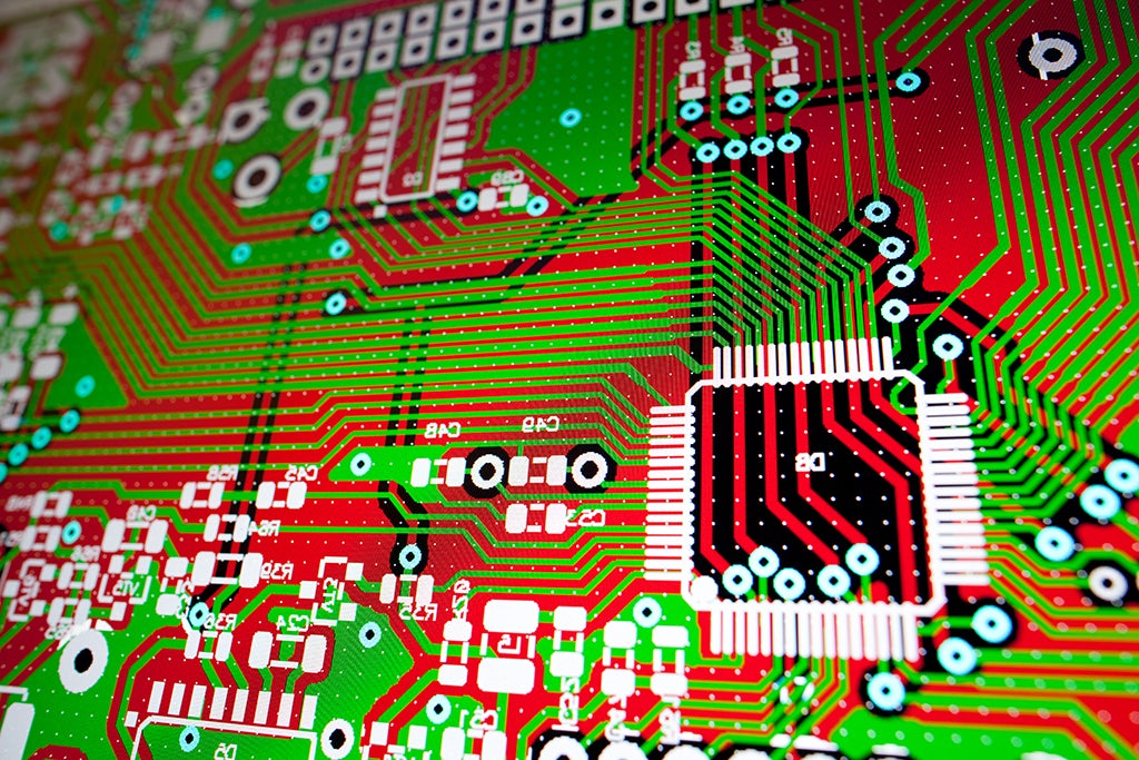
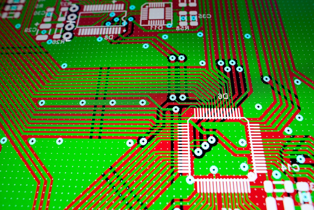
Across many different designs, designers will have to manage thousands (or more!) of PCB footprints.
PCB footprint creation is a delicate yet necessary step during electronics development, and it affects the quality of the layout and assembly. For especially complex boards, designers may encounter BOMs with component counts well in the thousands, some of which require unique footprints. Ultra Librarian can expedite this process by automating footprint creation and integration with your ECAD tool; PCB library maintenance is a cinch with a library of millions of verified components.
Working with Ultra Librarian sets up your team for success to ensure any design is going through production and validation with accurate models and footprints to work from. Register today for free!


")
