
IPC 7351 is the standard for surface mount component footprints
One of the most crucial aspects of PCBA design that can simultaneously be the most difficult to perform is the creation of component footprints and landing patterns. Designing landing patterns for through hole components are simple enough, although proper annular ring size and drill hole aspect ratios must be correct. SMD footprints, however, can be more complicated.
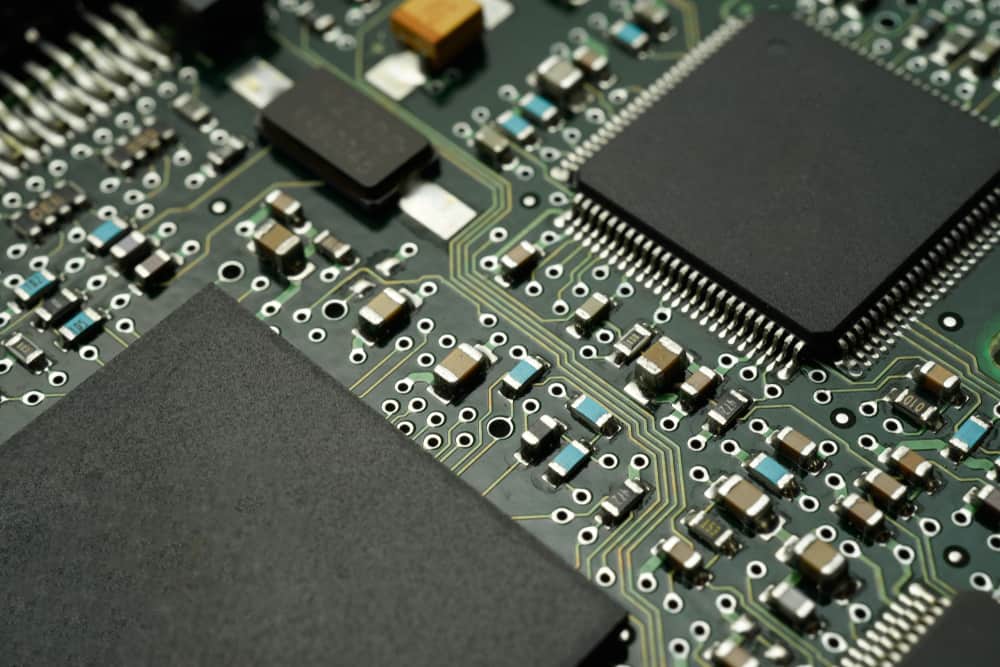
Surface mount components are only attached to the board’s surface; therefore, failing to achieve precise alignment can result in several manufacturing and performance issues. Additionally, there are limitations and constraints on component attributes, such as pin size, pitch, and separation, that must be adhered to. These constraints stipulated in the IPC 7351 standard are in place to ensure that fabricators and assemblers can create structurally sound and reliable board constructions.
Challenges of SMD PCB Footprint Creation
There was a time when being a good PCBA designer required creating accurate footprints from schematics or drawings, such as the one below, from the manufacturer datasheet.
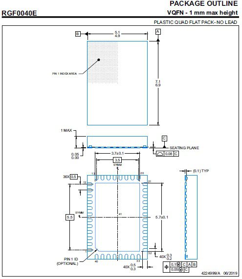
SMD footprint example for the MCF8316a sensor
Creating component footprints manually or from scratch is easier due to the ECAD tools available. Nevertheless, as listed below, there are still significant issues that must be addressed before your board design is ready for the manufacturer.
Common PCB Component Footprint Design Issues
- Component dimension accuracy
Electronic components come in all shapes and sizes. These dimensions are determined solely by the component manufacturer. Often a standard package size–such as 0402 for passives or SOT for ICs–is used, which is extremely helpful for ensuring part dimensions are accurate. Depending upon your design software, a common packages may be available.
- Pin attributes
For SMDs, pins, pads, or balls may be used to connect the component to traces. These connectors may be various sizes and shapes as specified by the manufacturer. Additionally, there is the pitch and spacing between pins and all of these parameters must be accurate.
- Pin and pad alignment
One of the most common issues that affect the PCB assembly of your board and less than optimal performance is misalignment between component pins and footprint pads. If severe enough, this design flaw can lead to solder bridging and/or shorts.
- Via type and locations
Multilayer PCB stackups and vias enable the design of compact boards, which has aided in the expanded applications for electronics over the last decades. However, it is critical that the best via type, size and location is chosen and that it aligns with your component pad or ball grid array.
- Reference indicators, markings and labels
Footprints or landing patterns are not complete without adequate and accurate markings. These may include pin 1 indicators, polarity marks, reference identification and labels.
The list above includes important parameters and considerations when creating component footprints. The absence of these may slow the development process or render your design unmanufacturable without modification or redesign. Therefore, all footprint creation should follow the IPC 7351 standard to avoid these contingencies.
What is the IPC 7351 Standard?
In 1957, the Institute for Printed Circuits (IPC) was founded to develop manufacturing standards for circuit boards. Since the organization–known today as IPC, International–has positioned itself as the premier standards organization for all aspects of PCBA production and testing. For example, committees of IPC have developed the following standards for PCB design, fabrication, assembly, and testing.
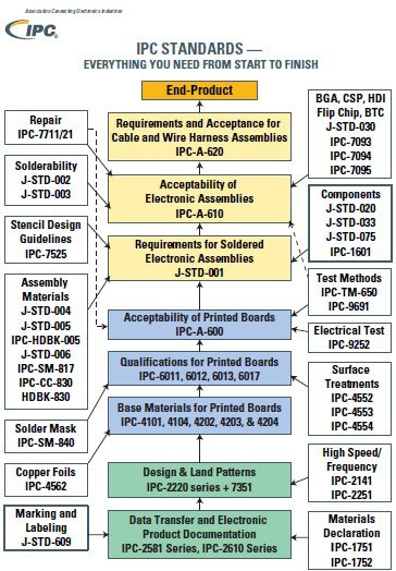
Summary of IPC Standards
In the figure above, yellow denotes PCB assembly standards, green represents board fabrication, blue is for design, and white for specializations within the three primary activities. Among the highlighted design standards is IPC 7351. The current version of this standard is IPC 7351B: Generic Requirements for Surface Mount Design and Land Pattern Standard.
IPC 7351 covers a lot of territory, but its main purpose is to provide circuit board designers with guidance for creating land patterns for passive and active components, whether from well-known package types or for designs from scratch. The standard is divided into 15 major sections or topics, which are listed below.
IPC 7351 Topics
- Scope
- Applicable Documents
- Design Requirements
- Component Quality Validation
- Testability
- Printed Board Structure Types
- Assembly Considerations for Surface Mount Technology (SMT)
- IPC-7352 Discrete Components
- IPC-7353 Gullwing Leaded Components, Two Sides
- IPC-7354 J-Leaded Components, Two Sides
- IPC-7355 Gullwing Leaded Components, Four Sides
- IPC-7356 J-Leaded Components, Four Sides
- IPC-7357 POST (DIP) Leads, Two Sides
- IPC-7358 Area Array Components (BGA, FBGA, CGA, LGA, Chip Array)
- IPC-7359 No-Lead Components (QFN, PQFN, SON, PSON, DFN, LCC)
- Zero Component Orientations
As the list indicates, the standard is divided almost in half with general design information and specific component type details. There are also a large number of figures and tables and even a land pattern calculator to aid you in creating PCB footprints that adhere to standard requirements.
How to Best Use the Standard For Creating Accurate SMD Footprints
Creating accurate SMD PCB footprints from scratch is a skill that is typically honed through experience. Fortunately, most parts manufacturers try to utilize standard package types for new product designs. This coupled with the availability of online CAD images and data; such as shown below, minimizes the cases where manual creation is necessary for landing patterns.
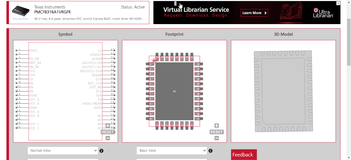
Verified CAD images from UL
However, it is good design practice to not only be familiar with IPC-7351 standards, but to also use them as guidelines when creating footprints for your components.
If you’re looking for CAD models for common components that adhere to the IPC 7351 standard, Ultra Librarian helps by compiling all your sourcing and CAD information in one place.
Working with Ultra Librarian sets up your team for success to ensure streamlined and error-free design, production, and sourcing. Register today for free.


")
