
 It is well-known that the work engineers do requires them to both read and design specifications that are detailed and accurate. A prime example of the importance of accurate specifications is when creating a schematic. Simply put, schematics are diagrams meant to explain how something is assembled or constructed so that it can be more fully understood. For PCB electrical and electronics engineers, this is an invaluable graphical tool for deciphering the operation of an electrical circuit. In order to grasp the importance of knowing how to read a circuit board schematic, it is informative to know the intent of utilizing schematics and the elements of which they are comprised.
Circuit Board Schematics and How They Are Used
Virtually every electrical or electronic system begins with the drawing of a graphical representation that includes the elements or parts included and how they are connected. For electrical systems—including residences or commercial structures—these drawings are often referred to as blueprints. Engineers and designers refer to these graphics as schematics. A typical example of a schematic is shown below.
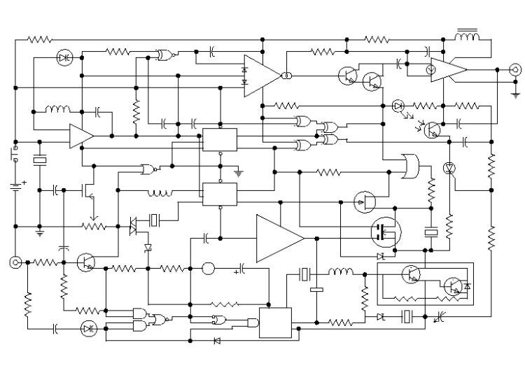
Circuit board schematic
Schematics may range from the complex, with densely packed components, to quite simple with a single part such as an antenna. For the development of PCBAs, circuit board schematics are utilized as follows:
Schematics provide the designer with a canvas with which to formulate an electrical layout that will perform the objectives of the design. This includes selecting all necessary components and defining interconnections or nets between them.
Creating schematics is not a simple process and often requires trial and error to arrive at the best or most useful design. Areas that can be the most troublesome are finding or having to create the right component symbol and ensuring all nets are connected and not overloaded.
Another fundamental requirement of the circuit board schematic is to ensure that all performance objectives are met. This may require circuit simulation to be performed to verify inputs and outputs and evaluate signal integrity. This is in addition to doing a design rule check (DRC) often to ensure that no design violations exist.
For PCB design software packages, the schematic provides the framework and initial layout of the board. This includes the footprints for the components, board dimensions, and ratlines—which are temporary lines showing connections between board elements and are used for autotracing and to help with your PCB layout design.
Not only is it important to know how your circuit board schematic is used, but it is also critical to understand what design elements it includes.
The Design Elements of A PCB Schematic
Just as the building of a PCBA proceeds through the steps of fabrication and assembly, the building of the PCBA graphic begins with the schematic and ends with the PCB layout. Therefore, a good way to view a circuit board schematic is as the first draft or the board layout. And some elements that are included on the layout are not present on the schematic—drill holes and vias, for example. However, schematics do contain the following elements:
- Component symbols
The most important elements of any circuit design are the components; it is imperative that the correct part library be used for each, as this is the source for the landing pattern or PCB footprint as well as other information that is used for the BOM.
- Reference designators
Another important element typically present on schematics is the reference designator which identifies the element—most often component—type. These are also very helpful for the PCB layout.
- Nets
Next to components, the schematic should contain all of the interconnections or nets needed for circuit operation. Omissions here will have an impact on how or whether your board works as it is intended.
- Annotations
As schematics may need to be read by others (for example, your manufacturer) or at a later time, it is a good idea to include any important textual information, such as changes that have been instituted.
The importance of schematics to the development of electronic circuit boards and products cannot be overstated. However, making the best use of these graphics requires that you know how to read a circuit board schematic effectively.
How to Read a Circuit Board Schematic With Purpose
Throughout the PCBA development process, which includes design, manufacturing, and testing, the ability to read and understand PCB diagrams is essential. This begins with knowing how to read a circuit board schematic effectively. This can be done by following the guidelines below.
How to Read a Circuit Board Schematic Effectively
- Understand the purpose and use for the schematic.
- Be able to identify the design elements .
- Be able to validate the schematic’s veracity.
A schematic is only as useful as it is accurate. One of the best ways to ensure that you acquire an accurate schematic is to utilize a schematic haven where the information is complete and vetted.
If you’re looking for CAD models for common components or design tips, such as how to read a circuit board schematic effectively, Ultra Librarian helps by compiling all your sourcing and CAD information in one place.
Working with Ultra Librarian sets up your team for success to ensure streamlined and error-free design, production, and sourcing. Register today for free.


")


