Apple founder Steve Jobs once said, “Technology is nothing. What’s important is that you have faith in people, that they’re basically good and smart, and if you give them tools, they’ll do wonderful things with them.” In making this statement, Steve was not dismissing technology. On the contrary, he was claiming if we are given the proper tools, we can push technological advancements to wonderful new heights.
Electronics engineers and designers are responsible for most of the recent advances in technology, including the computers and smartphones Steve’s company created. To design these advancements, many engineers rely on ECAD tools, which are the means by which 2D and 3D electronic component models are used to design schematics, PCBAs, and systems.
Let’s explore these tools further by defining what is ECAD, how it is used, and how to select the best tool for your next project.
What is ECAD?
Prior to discussing the usage and importance of ECAD for electronics design, it is helpful to define a few terms.
| Definitions:
Computer-Aided Design (CAD) – the utilization of computers to design, modify, and/or analyze a design, typically with the objective of optimization for a set of defined criteria. Electronic Computer-Aided Design (ECAD) – the creation and/or analysis of electronic components, integrated circuits (ICs), modules, printed circuit boards (PCBs), PCB assemblies (PCBAs), and/or electronic systems using computer software. Computer-Aided Design (CAD) File – for electronics design, a file generated with ECAD software that includes the data, text, and illustrations necessary to manufacture an electronic device, board, or system. |
The importance of ECAD cannot be overstated. Virtually every electronic device, product, appliance, or system in use today was designed with an ECAD software tool.
How is ECAD Used for Electronics Design?
Electronics products and systems are so named due to the inclusion of circuit boards or PCBAs, which are composed of electronic components and circuits. The design of a PCBA using ECAD software is a sequential process, consisting of the following steps:
- Schematic Generation (Capture)
- PCB Layout
- Simulation
- ECAD/MCAD Integration
1. Schematic Generation (Capture)
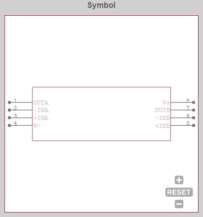
The first step for all the most simplistic designs is to create your schematic, where the component symbol—an example is shown in Fig. 1, below—is acquired during component selection. The symbol is then placed directly in schematic sheets and connected to other components with nets.
This is probably the most creative aspect of the design process and may include quite a bit of arrangement to ensure accurate connectivity between parts. It is also a good idea to attempt to arrange components, at least generally, as you anticipate they will be on the actual board. Doing so may simplify your PCB layout, especially for manual routing, but also if you use auto-routing (a common function with ECAD tools).
2. PCB Layout
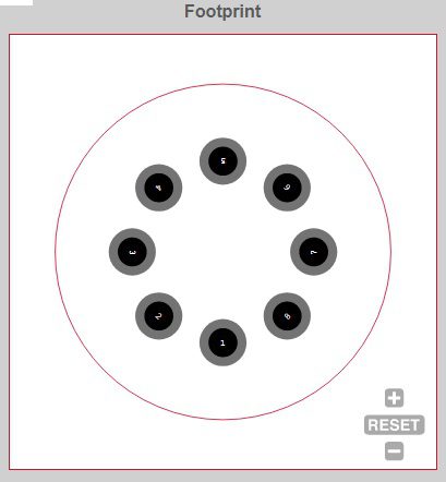
Most often, the second step in the design process is the layout. This includes placing components, trace routing, and defining board parameters such as size, materials, location of vias, and the number of layers and their properties. Both the schematic and layout are dependent on your parts library for schematic symbols and PCB footprints. A footprint example for the LM155 Op-amp (above) is shown in the figure below.
3. Simulation
Although it is not incorporated in all PCB design packages, another important ECAD capability is simulation. Schematics and PCB layouts may be simulated. The most used simulation tool for schematics is PSpice—an integral part of Cadence’s PCB Design and Analysis package—which requires your parts have a SPICE model library and is typically used for signal analysis. Board designs are also simulated, most often for power distribution (PDN) design and thermal analysis.
4. ECAD/MCAD Integration
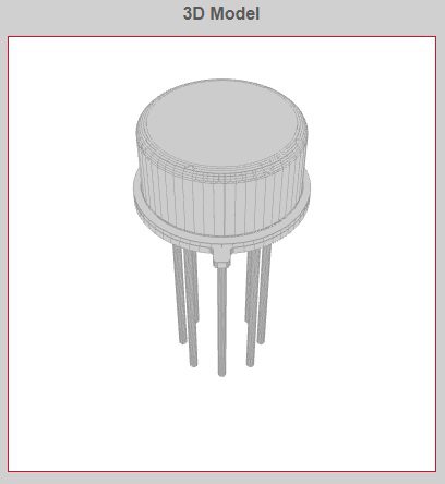
If you are working on a system design, the ability to create 3D drawings of components—as shown in Fig. 4, below—and boards is a definite asset.
The advantages of this capability are as follows:
- Inspection of component vertical clearances
- Inspection of stackup and via alignments
- MCAD or internal design of enclosures, cases, etc.
- Export for MCAD incorporation
How to Choose the Best ECAD Tool for Your Design
An ECAD tool should possess some basic functionalities and capabilities such as the ability to create the schematic and board layout and check for design errors. However, for the best and most efficient electronics design, there are other essentials that should be included in your ECAD tool. Among these are the ability to import and export commonly used design formats (including CAD file formats), back annotate between the schematic and PCB layout to ensure changes in one will reflect in the other, and create part symbols and footprints.
However, the most important ECAD function is the electronic part search, as the components selected will define functionality and operation, influence layout decisions and physical dimensions, and enable the optimization of your design prior to sending it off for manufacturing. Therefore, the best ECAD tool should provide for simple and easy component library integration into the design process. A good example of the advantages of this functionality are illustrated in the video, BOM creation.
Ultra Librarian, the premiere component library tool, integrates easily with many popular ECAD applications to help optimize your electronics design process. Working with Ultra Librarian sets your team up for success to ensure any design is going through production and validation with accurate models and footprints to work from. Register today for free.