
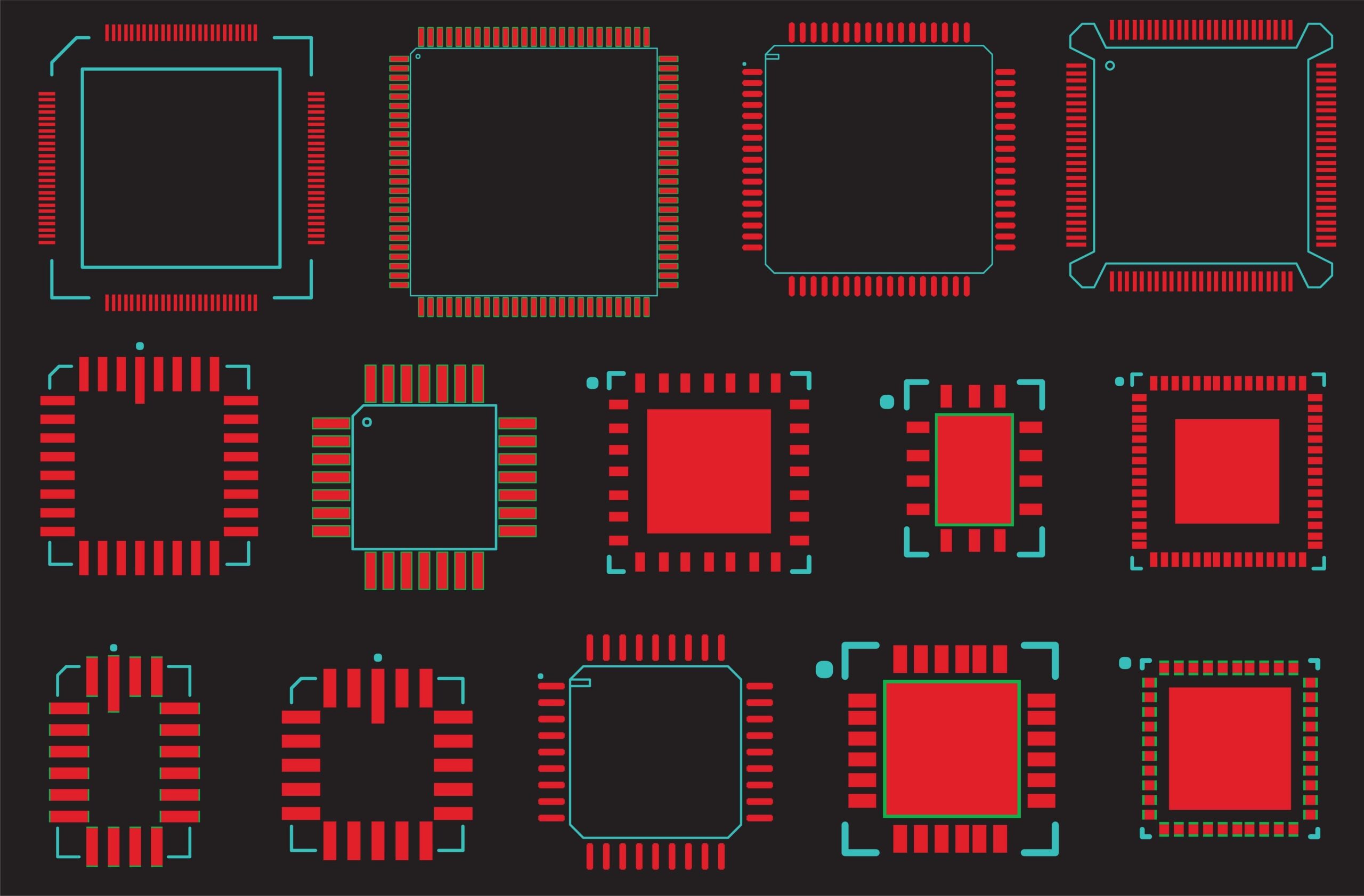
Electronic components have various footprint dimensions
“What is the key to avoiding the time and cost drains of what can seem like endless redesign and respins to achieve a production-ready PCBA design?” The answer to this question, from many of the most efficient PCB designers and engineers, would be to ensure the accuracy of your component library. Understanding this answer requires knowing the elements that comprise these libraries.
As the name implies, a component library is an ordered collection of the data and information needed to adequately define a part for design, procurement, and manufacturing. The best PCB design software tools include extensive libraries that include information like MPNs, links to datasheets, and are integrated with real-time data to help you avoid supply chain disruptions. However, all include part symbols for schematic capture and the footprints that are essential for PCB layout design, fabrication and assembly.
Every component has a PCB footprint. And footprints come in all shapes and sizes. The accuracy of your part’s footprint dimensions is critical to ensure your board can be built and that it functions as intended.
What Are PCB Footprints?
As shown for the IR2110 below, PCB footprints, along with schematic symbols and 3D models, are the most common graphical representations of components used for electronic computer-aided design (ECAD) and manufacture of PCBAs.
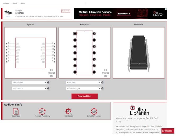
Schematic, footprint and 3D model for the IR2110 from UL
For all but the simplest of designs, schematic symbols are necessary to help define the net connections between components. Symbols are also important when performing pre-layout simulations; to analyze circuit operation and performance. And with the thrust toward ECAD-MCAD co-design, 3D CAD models are becoming more important for PCB designers. However, 2D PCB footprints are comprised of the most critical elements for board layout and build.
PCB Footprints vs Landing Patterns
PCB footprints are often, mistakenly, used interchangeably with landing patterns. However, there are distinct differences between these two PCB layout component parameters.
As shown above, the landing pattern provides important information for board fabrication. This includes areas where copper should remain after etching; such as surface mount part pad and thermal relief locations. In contrast, the footprint defines the component imprint on the surface of the circuit board, which includes via locations for through-hole parts and solder mask layer markings, which are important for PCB assembly.
Footprint dimensions, which are always smaller than corresponding landing patterns, are defined by actual component size. Examples include 0805, 1206, and 1210 that are common for passive components. Constraints on footprint dimensions, as well as landing patterns, are provided by industry standard IPC 7351. Adhering to these rules and guidelines is essential for a successful board build, as is ensuring the accuracy of footprint dimensions.
Optimizing the Accuracy of PCB Footprint Dimensions
PCB design and manufacturing depend on the accuracy of footprint dimensions. These specifications dictate the best locations for components to adhere to PCB spacing requirements and minimize the negative effects of EMI and EMC. Footprint dimensions are also critical for automatic pick and place machine operation during the assembly of your boards. Meeting these mandates is best accomplished by following guidelines, as listed below.
The importance of ensuring the accuracy of your footprint dimensions cannot be overstated. Failing to meet this criterion will result in longer than necessary PCBA development turnaround time and avoidable additional costs.
If you’re looking for CAD models for common components or important design information, like how to ensure your footprint dimensions are accurate, Ultra Librarian helps by compiling all your sourcing and CAD information in one place.
Working with Ultra Librarian sets up your team for success to ensure streamlined and error-free design, production, and sourcing. Register today for free.


")