
PCB reference designators
One of the often underutilized tools in a PCB designer’s toolbox is the silkscreen. This top layer of the PCB layout is where component footprints are placed, and is critical for accurate component placement during PCB assembly. However, this is not the only function of the silkscreen. Another important usage is for fiducials, including PCB reference designators which are important throughout PCBA development and once boards are deployed.
What Are Reference Designators?
Circuit boards include different types of markings used to aid the development process, including:
Fiducial marks are used by the pick-and-place machine during assembly to align the board so component placement can be done precisely. They are indicated by the red arrows in the figure below.
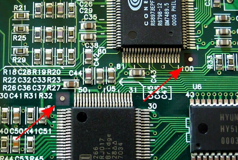
Fiducial marks on a PCBA
Pin 1 indicators are typically used to specify the first pin for ICs to ensure the correct orientation, and thus connections for these components. It is important to note that while it is not common, pin numbers are sometimes used for other components as well.
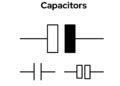
Polarity indicators are often used for passive components, such as capacitors and diodes, where the direction of voltage drop or current flow is imperative for operation.
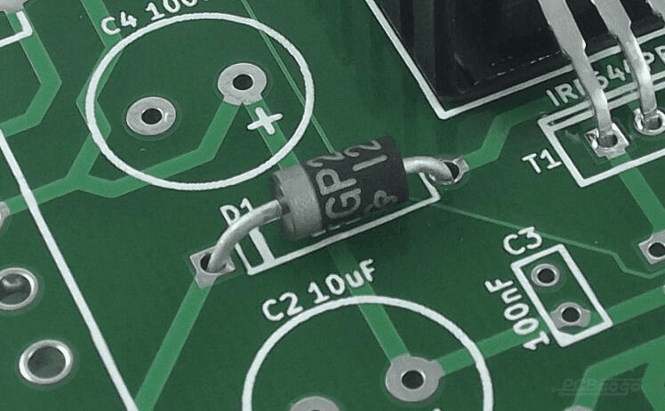
Polarity reference indicator. Image from PCBgogo
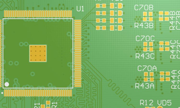
Reference designators are used to specify an assembly, subassembly, component, or other element type. These markings are placed on the silkscreen of a circuit board to aid in identifying where a particular component or element is located and that the specification—in the case of components—matches what is given in the board’s BOM.
PCB assembly with reference designators
In contrast to the other markings used on circuit boards, PCB reference designators are standardized by ASME Y14.44-2008, Reference Designations for Electrical and Electronics Parts and Equipment. This standard is intended to provide a uniformly recognized format for reference designators, including three methods to achieve this: a location method, a location coding method, and a unit numbering method.
Which PCB Reference Designators Should You Know?
The most common means of implementing PCB reference designation is by using the unit number method or component code, where each component is identified by a type abbreviation and a specific number. Common types are listed in the table below.
| TABLE OF STANDARD PCB REFERENCE DESIGNATORS | ||||
| Reference Designator | PCB Element | Reference Designator | PCB Element | |
| A | Assembly | PS | Power supply | |
| AN, AS | Antenna | Q, TR | Transistor | |
| AR | Amplifier | R | Resistor, potentiometer | |
| B | Battery | RT | Thermistor | |
| BR | Bridge rectifier | RLA, RY | Relay | |
| BZ | Buzzer | S, SW | Switch | |
| C | Capacitor | TP | Test point | |
| CB | Circuit breaker | TR | Transistor, transducer | |
| D | Diode | U | IC, inseparable assembly | |
| M | Meter, measuring device | W | Cable, wire, busbar | |
| MH | Mounting hole | XTAL | Crystal rectifier | |
| OP | Operational amplifier | XMER | Transformer | |
| P | Plug | Y | Crystal oscillator | |
The list above is not exhaustive. For a complete listing, please see the ASME Y14.44-2008 standard.
Why Are Reference Designators Important?
PCB reference designators are one of the tools that can be utilized to improve a design throughout development and even after deployment. For design, designators are impactful for organizing your schematic and netlist connections. For assembly, these markings ensure components are placed on the right footprints and are oriented correctly. During testing, designators, such as test points, are vital to analyzing operation and performance. And, in the unlikely event your board fails after installation, reference designators ensure the correct components are replaced.
If you’re looking for CAD models for common components, including accurate data to ensure your PCB reference designators match your BOM, Ultra Librarian helps by compiling all your sourcing and CAD information in one place.
Working with Ultra Librarian sets up your team for success to ensure streamlined and error-free design, production, and sourcing. Register today for free.


