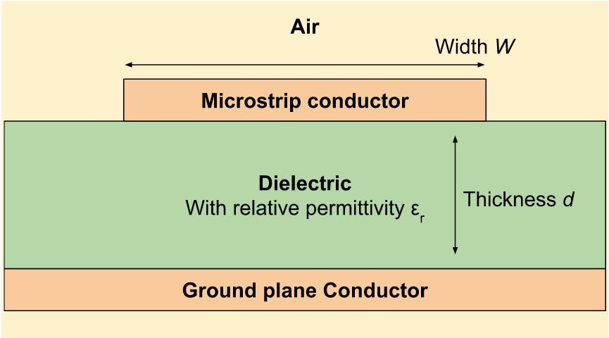
Simple diagram of a microstrip conductor and relevant PCB layers
The demand for high-speed, high-frequency communication systems in electronic devices is ever-increasing. As a result, the design and performance of microstrip transmission lines have become pivotal in ensuring signal integrity and that PCBs function as designed. For this reason, the effective simulation of microstrip transmission lines is a critical step in optimizing their design and performance. Microstrip transmission lines are widely used in printed circuit boards to carry high-frequency signals. These lines consist of a conductor trace on the top layer of a PCB, separated from a ground plane beneath it by a dielectric substrate. The design and routing of microstrip transmission lines must consider a range of factors, including signal frequency, impedance, and crosstalk, making simulation an invaluable tool for engineers.
Simulation of Microstrip Transmission Line Tips Summarized
Importance of Simulation
Simulation plays a critical role in designing and optimizing microstrip transmission lines for several reasons:
- As signal frequencies increase, the electromagnetic behavior of transmission lines becomes more complex. Factors such as signal reflection, dispersion, and crosstalk at high frequencies become significant. Simulation enables engineers to predict and mitigate these issues during the design phase.
- PCB fabrication can be costly, and design errors can lead to expensive rework. Through simulation, engineers can iterate and refine their designs virtually, reducing the risk of costly mistakes during the manufacturing process.
- The primary goal of microstrip transmission line design is to ensure signal integrity – the ability of a signal to retain its quality from source to destination. Simulation allows for fine-tuning parameters like trace width, dielectric material, and layer stackup to minimize signal degradation.
Best Practices for Microstrip Transmission Line Simulation
To simulate microstrip transmission lines effectively, engineers should follow best practices and employ the right simulation techniques and tools. Here are some essential guidelines to consider during simulation:
- Select a simulation tool that accurately models microstrip transmission lines. Widely used software packages offer robust capabilities for simulating high-frequency circuits.
- Ensure that the dielectric properties of the substrate material are correctly modeled in the simulation software. Specifically, taking note of important values such as relative permittivity and loss tangent is critical for accurate results.
- Use simulation to optimize the trace width to achieve the desired characteristic impedance for your microstrip line. Impedance matching minimizes signal reflection and loss.
- Consider the layer stackup of your PCB. Simulation can help determine the optimal arrangement of layers and the dielectric constant of each layer to achieve the desired performance.
- Perform signal integrity analysis to evaluate key parameters such as eye diagrams, jitter, and bit error rate. Simulation can help identify and rectify issues that could affect signal quality.
- Simulate crosstalk between microstrip traces and assess electromagnetic interference (EMI) to minimize unwanted coupling and noise.
- Account for temperature variations and environmental conditions in your simulation to ensure the design’s stability and reliability under real-world operating conditions.
PCB containing a microstrip.
Microstrip Characterization and Simulation Setup Tips
A typical microstrip configuration comprises a conductor with a width denoted as W, a dielectric substrate with a thickness of d, and a relative permittivity of εr. The dielectric, typically thin with a thickness significantly smaller than the wavelength (λ), concentrates the field lines primarily in the region between the conductor and the ground plane, although some portion extends into the air region above the conductor.
Designing your microstrip to achieve a specific characteristic impedance, such as 50 Ω at your desired frequency is important. Ensure that the electrical length is also set to correspond to the desired degree of phase delay. In your simulation software, set any necessary E-field and H-field monitors at the frequency of interest. Boundary conditions in all directions are primarily governed by “magnetic” rules, except below the microstrip, which can be treated as “electric,” simulating the ground plane. Setting a small spacing above the microstrip is also important to represent the air region. Parameters of interest include the thickness of the dielectric, width of the microstrip line, length of the transmission line, width of the dielectric substrate, and the thickness of the copper conductor.
Microstrip Trace Routing Tips
Once you’ve simulated your microstrip, keep in mind the following rules during routing:
- Keep a consistent trace width that is uniform along the entire length. Variations in trace widths can lead to impedance mismatches. Using a calculator to determine the most appropriate trace widths based on your target impedance, coupled with any relevant simulations you’ve done, may be helpful.
- Ensure a continuous and solid ground plane is on the layer adjacent to the targeted microstrip and avoid splits in the ground plane. If not, your simulation results may be inaccurate.
- Keeping microstrip traces short can help reduce signal propagation delay and distortion.
As you delve deeper into the intricate world of microstrip transmission line design and simulation, having the right tools at your fingertips is essential. If you’re looking for CAD models for common components used in any PCBs that may require a simulation of microstrip transmission line, Ultra Librarian helps by compiling all your sourcing and CAD information in one place.
Working with Ultra Librarian sets up your team for success to ensure streamlined and error-free design, production, and sourcing. Register today for free.