Following High-Speed PCB Design Guidelines can help you avoid costly respins
In the early days of electronics, printed circuit board (PCB) layout was often treated as “connecting the dots.” As long as the copper connected pin A to pin B, the circuit worked. Today, that approach is a recipe for failure. With modern processors, memory, and interfaces running at blistering speeds, PCB traces themselves act as transmission lines, where every millimeter of copper affects signal quality.
Success in this regime requires a shift in mindset from “connection” to “propagation.” Following high-speed PCB design guidelines is essential to prevent signal reflection, crosstalk, and electromagnetic interference (EMI), which can render a board non-functional. This guide covers stackup essentials, component placement, power integrity considerations, and routing rules required to master high-speed design, and concludes with real-world examples.
The Foundation: Layer Stackup and Materials
High-speed design is defined by signal edge rate, not clock frequency. When fast rise or fall times cause reflections to return before a transition completes, typically when trace length exceeds its critical length, the trace must be treated as a transmission line. At this point, a well-designed stackup is essential, as the layer stack forms the foundation of signal integrity and enables successful high-speed routing.
1. Controlled Impedance
High-speed signals require a constant impedance (typically 50Ω for single-ended and 90Ω or 100Ω for differential pairs) to prevent signal reflections. This is achieved by balancing the trace width, copper thickness, and dielectric height.
- Guideline: Work with your fabricator early to define the stackup. Use a field solver to calculate the specific trace widths required to achieve your target impedance on each layer.
2. Solid Reference Planes
High-speed signals propagate as electromagnetic fields between the trace and the reference plane.
- Guideline: Always route high-speed signals adjacent to a solid reference plane (Ground is preferred). Never route high-speed traces on two adjacent signal layers (broadside coupling) as this increases crosstalk and creates impedance discontinuities.
3. Material Selection
Standard FR-4 is sufficient for many applications, but at very high frequencies (typically >10GHz), its dielectric loss (Df) becomes significant.
- Guideline: Ensure the dielectric constant (Dk) is stable at your target high frequencies. For extremely high-speed designs, consider low-loss materials (like Rogers or Megtron). Additionally, specify low-profile copper to minimize skin-effect losses, and choose solder masks optimized to minimize the dissipation factor.
Component Placement and Routing Rules
Once the stackup is defined, the physical layout determines success.
1. Strategic Component Placement
Not all nets are equal. Identify your interfaces (DDR, PCIe, USB, Ethernet) and route them first.
- Guideline: Place the CPU/FPGA and the transceiver/connector to allow for the shortest, most direct routing path.
- Noise Management: Group components by function (analog vs. digital) to prevent noise coupling. Place your noisiest components, such as high-speed ADCs, in the center of the board rather than near the edges to reduce EMI radiation.
2. Differential Pairs
Differential signaling relies on the balance between the positive (P) and negative (N) traces to reject common-mode noise.
- Length Matching (Serpentine Routing): The most critical rule is intra-pair matching. If lengths differ, signals arrive at different times (skew). Use serpentine (meandering) routing to extend the shorter trace to match the longer one. Ensure the spacing between the meanders is at least 3x or 4x the trace width to prevent self-coupling.
- Coupling: Keep traces close together to maintain differential impedance, but avoid placing them so close that manufacturing tolerances cause impedance mismatches.
3. The Return Path (The Most Ignored Rule)
Current travels in loops. For every signal going out, a return current comes back directly underneath it on the reference plane.
- Guideline: Never route a high-speed trace over a split in the reference plane. Crossing a gap forces the return current to take a long, inductive loop around the split, acting as a slot antenna that radiates EMI and ruins signal integrity.
4. Crosstalk Reduction (The 3W Rule)
Crosstalk occurs when a signal on one trace couples energy onto a neighbor.
- Guideline: To minimize crosstalk, keep the center-to-center distance between traces at least 3 times the trace width (3W). For highly aggressive signals (like clock lines), increase this to 4W or 5W.
5. Power Integrity and Grounding
Clean power is just as important as clean signals. Voltage ripples can induce jitter in clock signals.
- Decoupling: Place decoupling capacitors as close as possible to the power pins of the IC. Use the smallest value capacitors closest to the pin to handle the highest frequencies.
- Simulation Strategy: Validation should occur in two stages: first, a pre-layout simulation is performed to model the circuit and set constraints (topology, termination). Next, a post-layout simulation (SI/PI analysis) is performed to verify that the physical routing, power distribution network (PDN), and thermal dissipation meet the design requirements.
High-Speed PCB Design Guidelines Checklist
| Category | Checklist |
| Routing | Are traces routed at 45° angles or curves? (Avoid 90° corners to prevent impedance changes). |
| Return Path | Did you verify that no high-speed trace crosses a split in the ground plane? |
| Crosstalk | Is the 3W rule applied to sensitive clock and data lines? |
| Vias | Are you using stitching vias next to signal vias when changing reference planes to maintain the return path? |
| Termination | Are series or parallel termination resistors placed correctly (close to the source or load, respectively) to minimize ringing? |
| Stubs | Are via stubs back-drilled or minimized on ultra-high-speed lines to prevent resonance? |
Common Pitfalls of High-Speed PCB Design
Applying these high-speed PCB design guidelines is critical in modern high-performance designs. For example, in a DDR4/5 memory subsystem, failing to length-match address and command buses within picosecond tolerances will prevent the memory controller from latching data. Similarly, in a 10Gbps Ethernet interface, a simple return path discontinuity caused by a via field can create impedance mismatches that result in total link failure due to signal reflection. More pitfalls include
- Crossing Split Planes: The most common cause of EMI failure is routing a high-speed trace over a gap in the reference plane (e.g., crossing from a 3.3V plane to a 1.8V plane without a stitching capacitor).
- Via Stubs: On ultra-high-speed lines (PCIe Gen 4/5), unused via barrels act as resonant stubs. If not back-drilled, they attenuate signals at specific frequencies.
- Improper Termination Placement: Placing series termination resistors too far from the source, or parallel termination too far from the receiver, renders them ineffective against ringing.
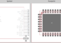
The first step in any high-speed design is ensuring your component footprints are accurate. An incorrect pad size can create parasitic capacitance, ruining the impedance profile. Ultra Librarian provides verified, IPC-compliant CAD models that ensure your high-speed components interact correctly with your PCB layout.
Working with Ultra Librarian sets your team up for success by ensuring streamlined, error-free design, production, and sourcing. Register today for free.


")