Power management in your IC design
Every electronic system, from a coin-cell-powered wearable to an industria
l server backplane, relies on a stable supply of power. It is the one subsystem that cannot fail without taking everything else down with it. Power management IC design involves converting raw, potentially unstable energy sources into precise voltage rails required by sensitive silicon.
Modern power management ICs (PMICs) are no longer just simple voltage regulators. They are sophisticated system controllers that integrate switching regulators (buck, boost), linear regulators (LDOs), battery management, and supervisory logic into a single package. For a hardware engineer, the challenge lies not just in selecting a chip but in optimizing for efficiency, thermal performance, and electromagnetic compatibility (EMC).
Essentials of Power Management IC Design
At the core of any PMIC architecture are the voltage regulators. The choice between topology types, specifically switching versus linear, dictates the efficiency and noise profile of the final design.
Switching Regulators (Buck/Boost)
Switch-mode power supplies (SMPS) use an inductor and rapid switching to store and transfer energy. A buck converter steps the voltage down, while a boost converter steps it up. These are the engines of modern electronics, often achieving efficiencies between 85% and 95%. However, this efficiency comes at a cost: noise. The switching action (typically 300 kHz to several MHz) generates voltage ripple and electromagnetic interference (EMI) that can couple into sensitive signal paths.
Linear Regulators (LDO)
Low Dropout Regulators (LDOs) operate purely resistively. They burn off excess voltage as heat to maintain a steady output. While this makes them inefficient for large voltage drops (e.g., 12V to 3.3V), they are electrically quiet and react almost instantly to transient load changes. This makes them ideal for powering analog sensors, PLLs, or RF front-ends where noise is the enemy.
The following table summarizes when to deploy which power management topology:
| Feature | Buck Converter | Boost Converter | LDO (Linear Regulator) |
| Primary Function | Step-down voltage | Step-up voltage | Step-down voltage |
| Efficiency | High (85-95%) | High (80-90%) | Low (depends on Vin/Vout) |
| Noise / Ripple | Moderate to High | Moderate to High | Very Low |
| Complexity | High (Inductor + Caps) | High (Inductor + Caps) | Low (Caps only) |
| Best Use Case | High power, digital cores (CPU/FPGA) | Battery-powered LED drivers, USB OTG | Analog audio, RF, Sensors |
Calculating Efficiency
Understanding where power is lost allows engineers to mitigate thermal issues before they arise. Efficiency () is simply the ratio of power out to power in (n = P<sub>out</sub>/P<sub>in</sub>), but in design practice, it is often more useful to calculate the power loss (Ploss), as this determines the temperature rise of the die.
LDO Efficiency
For linear regulators, efficiency is dominated by the voltage differential. Under the assumptions listed below, the efficiency simplifies to:
Where:
$$P = I \cdot V$$
$$I_{in} \approx I_{out}$$
- Quiescent current (Iq) is negligible (true for moderate to high load currents)Quiescent current (Iq) is negligible (true for moderate to high load currents)
If you regulate 5V down to 3.3V, your maximum theoretical efficiency is 66%. The remaining 34% of energy is dissipated purely as heat.
Switching Regulator Efficiency
Switchers are more complex. Their total loss is primarily the sum of conduction losses (resistive energy lost while current flows) and switching losses (energy lost during the transition between on/off states).
- Conduction Loss (Pcond): Dominates at heavy loads. It is a function of the MOSFET’s on-resistance (RDS(on)) and the inductor’s DC resistance (DCR)$$P_{cond} \approx I_{out}^{2} \times (R_{DS(on)} + DCR)$$
- Switching Loss (Psw): Dominates at light loads or high frequencies. It occurs because the MOSFET cannot switch instantly; during the rise (tr) and fall (tf) times, voltage and current overlap, burning power.$$P_{sw} \approx \frac{1}{2} \times V_{in} \times I_{out} \times (t_r + t_f) \times f_{sw}$$
This creates a trade-off: increasing switching frequency (𝑓sw) reduces inductor size but increases switching losses. Conversely, choosing large MOSFETs with very low (RDS(on)) reduces conduction loss but often increases gate capacitance, which slows down switching and increases switching loss.
Layout: Controlling Noise
In power management IC design, the schematic is only a theory; the layout is the reality. A perfectly simulated circuit can fail essentially if the physical board design ignores the physics of high-frequency switching.
The most common point of failure is the “hot loop.” In a buck converter, this is the path formed by the input capacitor, the high-side MOSFET, and the low-side MOSFET (or catch diode). When the switches toggle, the current in this loop changes from zero to several amps in nanoseconds. This high di/dt interacts with any parasitic inductance in the trace to generate voltage spikes (V = L di/dt), which ring out as EMI.
Layout Best Practices:
- Minimize the Loop Area: Place the input ceramic capacitor as physically close to the VIN and GND pins of the IC as possible. Every millimeter of trace adds parasitic inductance.
- Solid Grounding: Do not use thin traces for ground connections. Use a solid ground plane on the layer immediately below the top layer. This provides a return path for high-frequency currents and acts as a shield.
- Isolate Sensitive Nodes: The feedback (FB) pin is a high-impedance input looking for a stable voltage reference. Route this trace away from the noisy switch node (SW) and inductor to prevent noise coupling that causes output instability.
Component Selection
The Inductor
The inductor stores energy during the “on” time and releases it during the “off” time. Two specs matter most: Saturation Current (Isat) and DC Resistance (DCR).
If the inductor current exceeds Isat, the core saturates, and the inductance drops rapidly. This turns the inductor into a low-value resistor, leading to a runaway current spike that can destroy the MOSFET. A safe rule of thumb is to select an inductor where Isat is at least 30% higher than the maximum load current plus the ripple current.
The Capacitor
Ceramic capacitors (MLCCs) are the standard for input and output filtering due to their low ESR (Equivalent Series Resistance). However, Class 2 dielectrics (like X5R and X7R) suffer from the DC Bias Effect. As you apply a DC voltage across the capacitor, its effective capacitance drops.
For example, a 10µF 16V X5R capacitor might only provide 2µF of effective capacitance when operating at 12V. If you fail to account for this derating, your control loop may become unstable, or your output ripple may exceed specifications. Always check the “Capacitance vs. Voltage” curve in the datasheet.
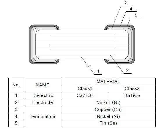
Structure of an MLCC capacitor
Sequencing and Protection
Modern systems require multiple voltage rails to turn on in a specific order. A high-performance FPGA might need its core voltage (0.8V) to stabilize before its I/O voltage (3.3V) is applied. If this sequence is violated, the chip could enter a latch-up state, drawing excessive current and potentially burning out.
PMICs handle this via sequencing. You can program the delay between rails using external capacitors or digital commands (I2C/PMBus).
Beyond sequencing, quality power management IC design includes built-in “safety nets”:
- UVLO (Under Voltage Lockout): Prevents the chip from trying to switch when the input voltage is too low, which would cause the internal MOSFETs to operate in their linear region and overheat.
- OCP (Over Current Protection): Monitors the current through the inductor or FETs. If a short circuit occurs, the PMIC enters “hiccup mode,” periodically trying to restart rather than burning itself out.
- OTP (Over Temperature Protection): Shuts down the regulator if the die temperature exceeds a safe limit (usually around 150°C).
Practical Design Examples and Tools
The approach to PMIC design shifts based on the application.
Scenario A: Battery-Powered Wearable
- Goal: Maximize battery life.
Solution: Use a PMIC with low quiescent current (Iq). You might accept a slightly higher ripple to use a PFM (Pulse Frequency Modulation) mode, which skips switching pulses at light loads to save power. You would likely use a tiny Wafer Level Chip Scale Package (WLCSP) to save space.
Scenario B: Industrial Motor Controller
- Goal: Reliability and thermal management.
- Solution: Efficiency is prioritized to reduce heat. You would choose a synchronous buck controller with external MOSFETs (to handle high current) and a lower switching frequency (e.g., 300 kHz) to minimize switching losses, even though it requires larger inductors.
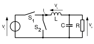
Synchronous buck converter circuit diagram
Simulation Tools
Never solder a board without first simulating it. Tools like LTspice, TINA-TI, or vendor-specific web tools (like TI’s WEBENCH or Analog Devices’ LTpowerCAD) allow you to verify efficiency, loop stability, and transient response.
For component selection, use tools like Murata SimSurfing or TDK SEAT to visualize the actual behavior of capacitors and inductors under load and bias, rather than relying on the nominal values printed on the box.
Designing a well-thought-out power architecture requires balancing conflicting requirements, and effective power-management IC design is crucial to achieving that balance. By validating designs in simulation, laying out switching regulators with intention, and derating components conservatively, engineers can ensure real-world reliability. Ultra Librarian improves this process by delivering accurate, manufacturer-verified symbols and footprints directly into popular ECAD applications, while providing easy access to parts from worldwide distributors to help accelerate sourcing and reduce design risk.
Working with Ultra Librarian sets your team up for success, ensuring streamlined and error-free design, production, and sourcing. Register today for free.