
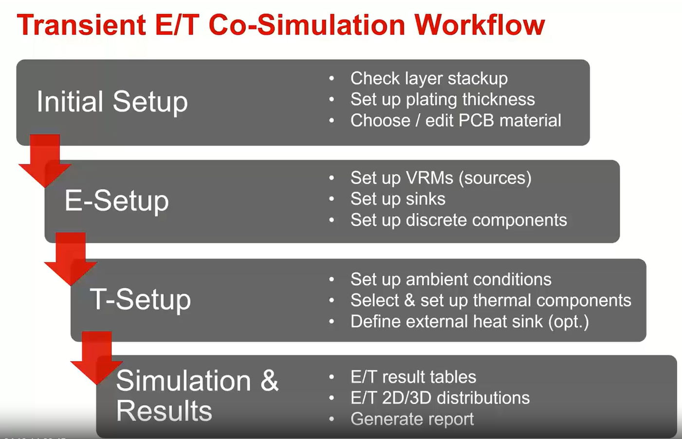
Transient electrical/thermal co-simulation workflow for high current PCB power design
Designing printed circuit boards (PCBs) with high power PCB design guidelines presents unique challenges in both electrical performance and thermal management. In a recent webinar hosted by STMicroelectronics and EMA Design Automation, experts walked through their collaborative flow for optimizing a three-phase inverter reference board (EVAL-SDDrive101) dedicated to battery-powered motor control. Below is a structured recap of the key guidelines, methodologies, and best practices covered for high-current PCB design guidelines.High Current Application Context
Battery-powered applications such as cordless vacuums or portable power tools often demand tens of amperes through the motor inverter stage to deliver hundreds of watts. Yet these systems are shrinking for portability, driving up power density and exacerbating both electrical and thermal design constraints.- Typical currents: 15 A RMS continuous, up to 50 A RMS with heatsink
- Supply voltage: up to 75 V
- Power density concerns: high currents in compact PCBs concentrate losses and hot spots
Layer Stack-up and Copper Planning
A four-layer PCB stack-up with heavy copper is the foundation of high-power PCB design guidelines:- Copper thickness: recommended 70 µm (2 oz) on both top and bottom layers
- Inner layers: balance between copper pour for current spreading and signal routing
- Via arrays: dense via stitching under power MOSFETs’ exposed pads to improve heat and current transfer through the board
Power Trace and Plane Design
Current Carrying Capacity
- Trace sizing: start from IPC-2221 standard guidelines (e.g., mm of width per ampere at given copper thickness), then refine via simulation
- Multi-layer replication: route power paths across all four layers to reduce overall parasitic resistance and distribute current density
Loop Minimization
- Switching node loops: tightly route high-di/dt switching loops (half-bridge switch node to return) to minimize loop inductance, reduce EMI, and improve switching performance
- Shunt placement: embed current shunts near the power stage in either three-shunt or single-shunt topology, ensuring short, low-inductance connections
Thermal Management Strategies
| Section | Parameter | Specification / Details |
| Component Placement | MOSFET orientation | Group high-power MOSFETs centrally, maximize copper area under exposed pads, cluster for uniform heat spreading |
| Heat sink interface | Ensure minimal thermal-resistance path from MOSFET junction to bottom-side heatsink via thermal vias and copper pours | |
| Thermal Via Design | Via diameter | Recommended 12 mil plated (not filled) for power-stage thermal vias |
| Via arrays | Recommended to place under MOSFETs and along power rails to balance top/bottom temperature (typical ΔT < 5 °C) | |
| Material Selection | Substrate | Standard FR-4 rated to 130 °C Tg |
| Heatsink readiness | Anticipating heatsink attachment on the bottom; design for efficient through-board conduction |
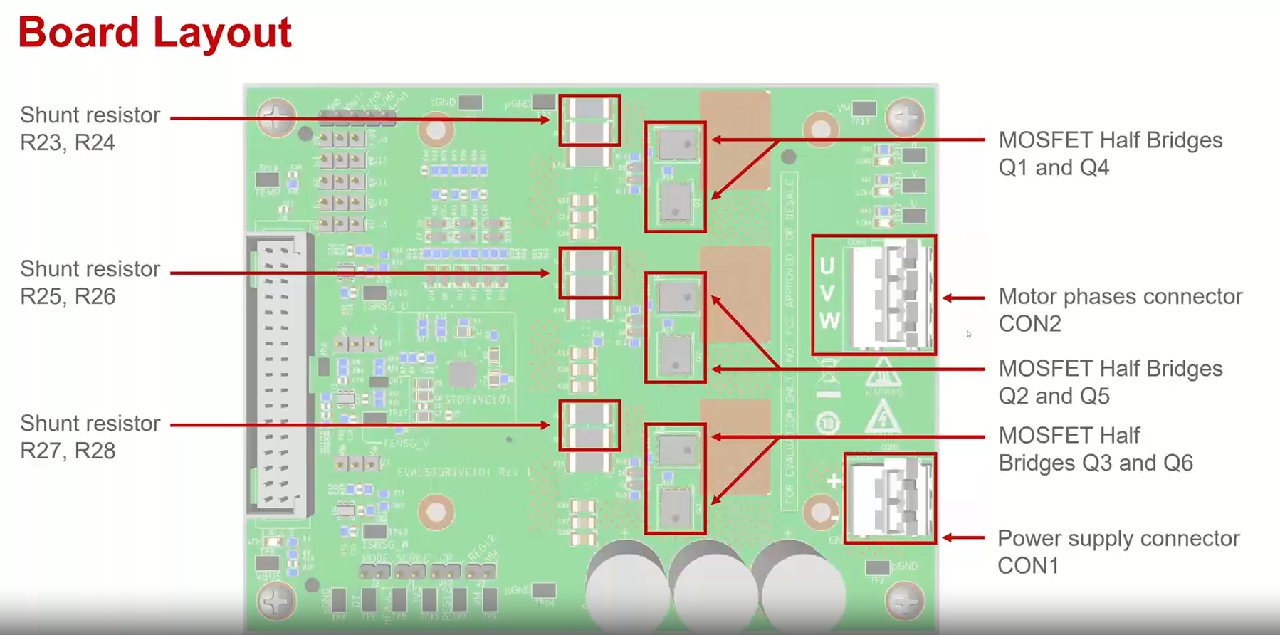
Board layout example for three-phase inverter reference board
Early-Stage Co-Simulation with Celsius
The Celsius environment facilitates rapid exploration of advanced scenarios without extra prototypes:- Heatsink modeling: add bottom-side heatsinks or individual component sink attachments to assess cooling benefits
- Material comparisons: swap FR-4 for high-TG or thermally enhanced laminates to quantify performance gains
- Copper fill or mask openings: simulate the impact of exposing bare copper vs. mask on power pours for additional plating and lower resistance
- Electrical DC analysis – computes IR drops, current densities, via currents
- Thermal analysis – evaluates steady-state and transient heating
- Co-simulation – accounts for thermal feedback on electrical parameters (e.g., copper resistivity vs. temperature)
Simulation Steps For High Current PCB Design Guideline Adherence
- Initial setup: import board (ODB++ or native Allegro), verify stack-up, pad stacks, and material properties
- Electrical setup: define VRMs or current sinks as loads, include discrete resistances for FETs and shunts (e.g., 1 µΩ to avoid numeric issues), place voltage/current probes
- Thermal setup: set ambient (28 °C) and natural convection (heat transfer coefficients for top/bottom), assign thermal components (compact two-resistor models for MOSFETs, standard models for shunts), and define transient power profiles
- Constraints: set limits on maximum trace temperature, via current density, and plane temperature to flag violations during simulation
- Run simulations: DC runs complete in seconds; transient thermal requires minutes (e.g., 15 min for full warm-up to ~15 min real time)
- Analyze results: use 2D/3D plots for current density and temperature distribution, inspect hot spots, and validate against lab measurements
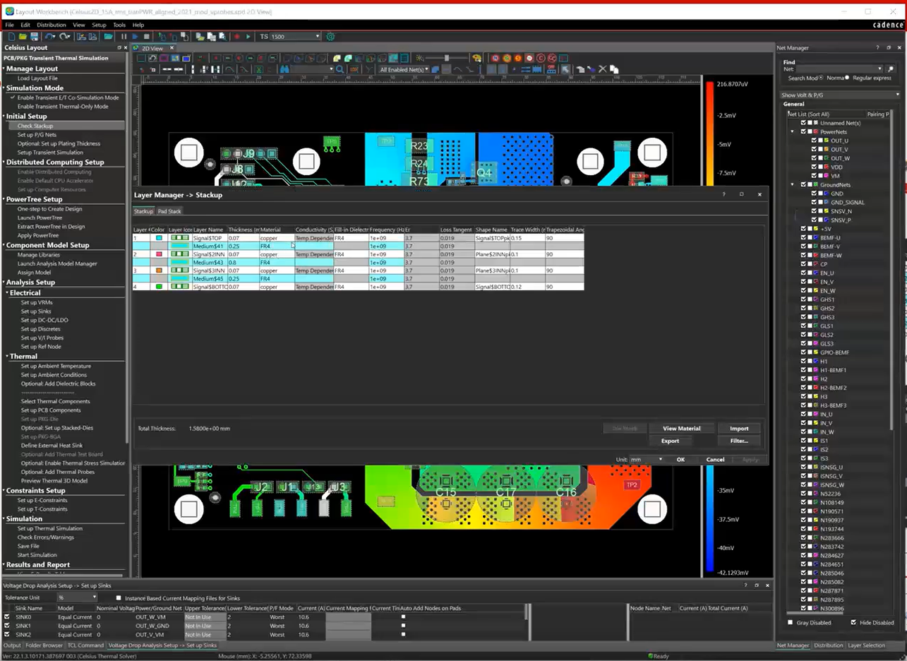
Celsius thermal simulation example with stackup manager
Simulation Results SDDrive101 Reference Board Example:
- Current density: average < 25 A/mm² on top layer, peaks under connectors and MOSFET pads, but well under stress limits
- Voltage drop: balanced across phases, negligible drop variance on the farthest phase trace
- Steady-state MOSFET junction temperature: ~95 °C (shunt ~86 °C) at 15 A RMS, matching thermal camera measurements within a few degrees
- Transient warm-up: board reaches > 90% of final ΔT within ~800 s (~13 min)
Iterative Layout Optimization
Based on simulation feedback, the team performed the following design revisions:- Area redistribution: enlarged copper pours, shifted thermal vias to eliminate bottlenecks
- Copper weight increase: moved from 1 oz to 2 oz on inner/outer layers for better spreading
- Channel balancing: refined trace routing to equalize electrical and thermal loads across phases
Important High Current Power PCB Design Guidelines
As the webinar example clearly illustrated, strategic simulation with a capable tool; such as Celsius, helps you optimize your board design efficiently. However, when designing high-current and/or high-power circuit boards, it is important to incorporate best practices, as shown below.
Guidelines for High Current/Power PCB Design
If you’re looking for CAD models for common components or high current/power PCB design guidelines, Ultra Librarian helps by compiling all your sourcing and CAD information in one place.
Working with Ultra Librariansets up your team for success to ensure streamlined and error-free design, production, and sourcing.Register today for free. - Early co-simulation of electrical and thermal performance dramatically reduces design cycles
- Heavy copper and via arrays are essential for managing high currents in compact PCBs
- Tight switching loops and balanced multi-layer routing minimize losses and EMI
- Data-driven layout refinements—guided by simulation—ensure targets of < 100 °C and safe current densities are met before the first prototype
- Simulation “what-if” testing cuts costs and time by avoiding unnecessary board spins


