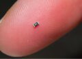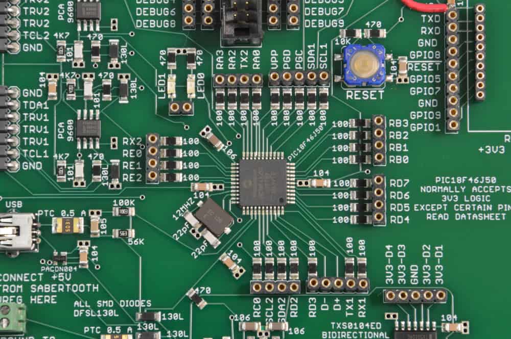
Close-up view of PCB component placement
How you arrange components on a printed circuit board (PCB) is vital for electronic device performance, reliability, and manufacturability. Where you place them impacts signal integrity, thermal management, electromagnetic compatibility, and other essential elements. Correct placement means reducing electrical interference and crosstalk and ensuring traces are routed efficiently so the board works correctly. It also helps to prevent overheating and improve system reliability. Taking the time to lay the components strategically is vital if you want the finished board to meet performance requirements, comply with industry standards, and reduce problems down the road.
Below is a table providing an overview of PCB component placement essentials.
PCB Component Placement Considerations
Let’s consider each PCB component placement element in more detail.
Component Size
Component size is a fundamental consideration. You should ensure that each component fits within its designated space on the board without interfering with neighboring elements.
Spacing
Maintaining strategic spacing between components is essential to prevent electrical interference and thermal issues. You can mitigate cross-coupling, EMI, and thermal hotspots by keeping distances adequate between sensitive components.
Routing
A key consideration in component placement is the efficient routing of traces. You should arrange components to create clear and organized signal paths to minimize signal distortion and maintain impedance control. This is critical for high-speed digital signals and radio frequency (RF) components.
Electromagnetic Interference
You should strategically position components to minimize electromagnetic emissions and EMI. Sensitive components may require additional shielding or isolation from high-frequency components.
Tolerances
Manufacturing tolerances should be considered to ensure precise placement during production. You should place components with enough margin to accommodate variations in the manufacturing process.
Signal Integrity
You should position PCB components to minimize signal distortion, reflections, and noise. To maintain signal integrity, you must follow best practices for high-speed digital signals, analog signals, and RF components.
Power Distribution
For maximum efficiency, you should design the power distribution network, including power and ground planes. Proper placement of power components and decoupling capacitors is critical for stable power delivery to all components.
Connector Placement
Connectors should be strategically positioned for ease of connectivity and accessibility. You should consider the mechanical stability of connectors, especially in applications where frequent plugging and unplugging may occur.
Crosstalk
Critical components should be placed apart, and sensitive traces should be routed away from high-speed or high-power traces to minimize crosstalk. You should use ground planes and proper signal layer stack-up to mitigate crosstalk.
Component Orientation and Density
You should align components for optimal functionality and space utilization and pay close attention to the orientation of polarized components and connectors. In addition, you should strive to balance the density of components so that available PCB real estate is utilized efficiently. Overcrowding should be avoided because it can lead to difficulties in routing and cooling.
Mounting Holes
The PCB should include mounting holes for stability and compatibility with enclosures or mechanical structures. You should place mounting holes to distribute mechanical stresses evenly.
Thermal Considerations
To address heat dissipation, thermal considerations play a significant role in component placement. You should strategically position heat-generating components and provide adequate ventilation so the PCB operates within specified temperature limits. This will result in components lasting longer and being more reliable.
In this article, we have provided a brief overview of key PCB component placement considerations. Still, the specific requirements may vary based on the project and the intended use of the PCB. You should always refer to the datasheets and guidelines provided by component manufacturers and adhere to best practices in PCB design.
How to Best Source PCB Components
A clear understanding of PCB component placement will aid you in designing and developing electronic boards and systems. With this knowledge, you can better source project components and devices.
If you’re looking for CAD models for common components or PCB component placement, Ultra Librarian helps by compiling all your sourcing and CAD information in one place.
Working with Ultra Librarian sets up your team for success to ensure streamlined and error-free design, production, and sourcing. Register today for free.