
Electronic Components:
Guide for Circuit Design & PCB Layout
It may seem that the process of building electronic circuit boards, which saw significant advancements during the last century, has not kept pace with the rapid and ever-escalating demands for PCBA functionality and performance. While the major manufacturing stages – fabrication and assembly–remain the same, the relationship between design and board spin has changed dramatically.
The most revolutionary change is the recognition by designers and manufacturers of the importance of abandoning the old black box development strategy and embracing a more open and integrated white box process for building circuit boards. The result is faster, better quality PCBA generation that accurately reflects the engineer’s design intent and aligns well with the CM’s equipment capabilities.
Achieving this highest level of PCBA development requires incorporating important considerations into your design process, including optimizing the selection of electronic components.

Your choice of components is the single most important defining activity that determines the quality of your PCBA design. Sourcing from reputable manufacturers is essential to avoid the time consuming pitfalls of choosing inferior quality parts, using incorrect symbols and footprints, or even being unaware of availability shortfalls or long turnaround times that may require redesign and increase design and development costs. These contingencies can be avoided by sourcing from the world’s largest component CAD library.
Essential Considerations for Good PCBA Design
Some PCB designers and engineers judge the quality of a design based on factors or metrics that are useful when creating the schematic or laying out the board. For example, minimizing the number of nets is helpful to simplify drawings, and ensuring all required pins are connected is critical for passing DRC checks when drawing schematics. Yet, neither of these affects the manufacturing process or the quality of the board build.
Ensuring that your circuit design satisfies its functional and operational objectives is critical. However, fulfilling these attributes does not encompass all the factors that determine the quality of your design. It is also essential to consider factors for manufacturability and reliability, as shown below.
Essential Considerations for Good PCBA Design
- Acceptable trace currents
- Accurate signal parameters
- Minimal EMI and good EMC
- Electronic components availability
- DFM rules and guidelines
- Regulation and standard compliance
- Material choices
For new product introduction or custom development, best practices for schematic capture and PCB layout should be followed.
Creating the Best Schematic Capture for Your Design
The first stage of PCBA design is to create the drawing of the circuit, which is called creating the schematic diagram or schematic capture. It is essential to use well-known symbols and design elements for the schematic as it is relied upon by other engineers and your manufacturer(s) as a graphical representation of your circuit and its connections. Schematics may be available online or copied from a datasheet for commonly used circuits.
For new and custom designs, you can use an online resource to build the schematic or create it from scratch with your CAD software tool. In either case, it is essential to consider manufacturability and reliability concerns, as shown below.
| SCHEMATIC CAPTURE FOR MANUFACTURABILITY AND RELIABILITY | |||
| Schematic Design Steps | Description | Incorporate Manufacturability Factors | Incorporate Reliability Factors |
| Step 1 | Choose electronic components | Ensure your supply chain is secure | Have a replacement parts resource |
| Step 2 | Get or create component symbols and place on schematic | Make sure symbols match footprints and BOM listing | |
| Step 3 | Get or create component footprints | Use standard package types, if possible | |
| Step 4 | Add other design elements | Choose readily available connectors and other parts | Use supplier mapping and real-time data |
| Step 5 | Create nets | Make sure all pertinent pins are fully connected | |
| Step 6 | Set up design rules | Follow your CM’s DFM and DFA rules | |
| Step 7 | Run DRC, if errors, make corrections and repeat Step 6 | Clear all errors | |
It may be pretty simple for some circuits to connect the schematic fully. However, partitioning the schematic drawing into sub-circuits for more complicated circuits, such as the evaluation board shown below, makes following the signal flow logic easier.
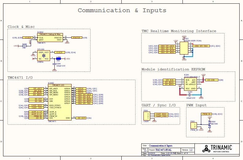
Triaminic TMC4671 evaluation board schematic. Image from
When creating your schematic, the most important issues are that the components meet your performance criteria, the symbol and footprint packages for your electronic components are accurate and match the parts listed in your BOM, and manufacturability and reliability factors have been incorporated. Once these mandates are met, the PCB layout can be done.
PCB Layout Design for Maximum First Pass Yield Rate Board Builds
PCB Layout Best Practices
-
Know and follow IPC standards for PCB layout.
-
Choose board material based on application.
-
If possible, use a standard board size and shape.
-
Set up design constraints based on your CM’s DFM rules and guidelines.
-
Arrange components based on signal type.
-
Use a consistent trace size and impedance.
-
Design your stackup to be symmetrical.
-
Run periodic error checks.
-
Use simulation to validate power distribution and thermal dissipation.
How to Best Optimize Your Electronic Components Selection Process
Optimizing your electronic components selection process is essential to creating the best PCBA design. This includes choosing both active and passive components and knowing when to opt for discrete parts. As the past couple of years has highlighted, it is also critical to have a plan for handling supply chain disruptions.
Researching components can cost you valuable development time and may not yield the best part for your project. The most efficient option is to employ a personalized component resource.
With Ultra Librarian’s Virtual Librarian Service (VLS) you can
- Minimize component search time and avoid errors like low quality or unavailable parts
- Encure CAD models are accurate and meet industry standards
- Make sure parts meet your company standards
- Streamline your embedded system design process
No single action will guarantee you never fall victim to a component shortage. However, as shown below, you can choose a proven reliable source for up-to-date, accurate, and manufacturer-verified CAD data and information to base your electronic component decisions.

Symbol, footprint, and 3D model of the TI_LM74800QDRRRQ1
That source is Ultra Librarian, the largest online parts library in the world, providing free parts and design resources to help you optimize your electronic components selection and create the best design.
If you’re looking for CAD models for common electronic components or design tips to help improve the efficiency of your PCB layout, Ultra Librarian helps by compiling all your sourcing and CAD information in one place. Working with Ultra Librarian sets up your team for success to ensure streamlined and error-free design, production, and sourcing. Register today for free.